Mathematical Modeling and Digital Control of A Hybrid Switching Buck Converter

Adv. Sci. Technol. Eng. Syst. J. 2(3), 937–945 (2017);
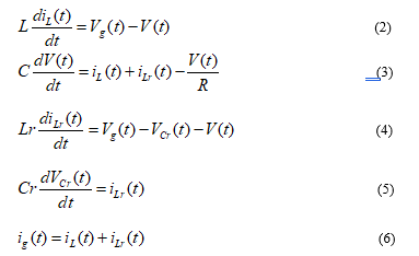
 DOI: 10.25046/aj0203118
The aim of this paper is to describe mathematical modeling and digital control of a hybrid switching buck converter. This converter belongs to a class of so called hybrid switching converters and contains a resonant capacitor, resonant inductor and a diode in addition to original buck converter components. The dc gain of this converter is shown to be independent of resonant branch parameters. Moreover the dc conversion ratio is derived for both ideal case and including main inductor dc resistance. Small signal model of the converter is derived and is shown to be similar to conventional buck converter. Simulation results in SIMPLIS Software as well as experimental results of digital control using an 8 bit STM microcontroller are presented. The potential advantages and applications of this converter are discussed.
1. Introduction
A new class of switching power converters known as hybrid switching converters has been proposed quite recently by S. Cuk [1], [2]. These converters embody the switching characteristics of two predominant methods of power conversion; square wave PWM switching converters and resonant switching converters. In square wave PWM switching converters, the reactive elements are charged and discharged linearly. Due to this, the semiconductor devices have to be hard switched resulting in significant switching losses. In order to avoid the switching loses, quasi resonant and resonant switching converters were developed. In resonant converters, the reactive elements are charged and discharged in sinusoidal manner resulting in ZVS or ZCS of semiconductor devices depending upon mode of operation. However, the resonant converters suffer from difficult design and control issues. In order to combine the best of the two worlds, a hybrid class of switching converters is proposed by [1], [2]. These converters are essentially derivatives of PWM switching converters and contain additional components as compared to their PWM method counterparts. These additional components, referred to as resonant components, provide capabilities otherwise impossible to achieve with either of the two classes of power converters [3]. The behavior of these resonant components is a hybrid of two methods: they either charge linearly and discharge in resonant manner or vice versa. These characteristics provide improvements over conventional PWM switching converters as will be shown in this paper.
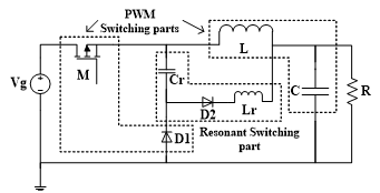 Figure 1 Hybrid Switching Buck Converter
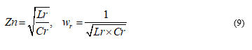
The paper is presented in the following manner: section 2 provides steady state operation and dc gain ratio of the hybrid switching Buck converter. Section 3 provides small signal derivation of HSBC and equivalent circuit is derived. Section 4 provides digital control implementation details around an 8 bit STM microcontroller. Section 5 gives simulation results performed in SIMPLIS software as well as practical example results. In section 6, possible applications of this converter are discussed.Figure 1 shows the hybrid switching buck converter (HSBC) with PWM switching parts and resonant switching parts highlighted. It can be seen that the converter is essentially a buck converter with additional resonant reactive components i.e. resonant capacitor Cr and inductor Lr along with a diode. The resonant capacitor Cr charges in resonant manner along with the resonant inductor Lr whereas it discharges linearly. The aim of this paper is to mathematically model the dc gain characteristics as well as small signal transfer function of this converter. It will be shown that this converter, though having a different dc gain ratio than a conventional buck converter, can provide similar characteristics as that of buck converter along with advantages such as magnetic size reduction of the main power inductor. Moreover, it is shown that the digital control of this converter can be achieved in a similar fashion as that of a conventional buck converter.
2. Steady State Operation and DC Gain Characteristics
The converter is assumed to be operating in continuous conduction mode. All semiconductor devices are assumed to be ideal. Also it is assumed that the resonant components (Cr and Lr) are much smaller than the main filter components (C and L). For simplicity of analysis, we assume that the on period of the main switch is equal to half of resonant period where resonant period is defined as:
![]() The converter operates in two modes depending on the state of MOSFET switch M. The resulting circuit waveforms along with the equations describing the reactive elements are presented next.
The converter operates in two modes depending on the state of MOSFET switch M. The resulting circuit waveforms along with the equations describing the reactive elements are presented next.
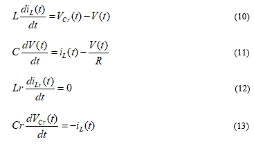
2.1 MOSFET Switch ON
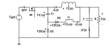 Figure 2 MOSFET ON, D2 ON, D1 OFF
When main MOSFET switch is ON, the diode D1 is reversed biased and diode D2 turns ON. The current flows from input to output charging both the main power inductor and resonant branch comprising of Lr and Cr. The capacitor Cr is charged resonantly. The inductor Lr is volt-sec balanced during this time interval only as the current through Lr flows only when D2 is conducting. This implies a different volt-sec balance approach than the main inductor L which is volt-sec balanced over complete switching period. It is assumed here that the resonant capacitor Cr is initially charged to a voltage level of Vcr1. The important waveforms and associated equations for this mode can be presented as:
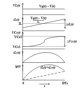 Figure 3 Waveforms in Mode I
 As can be seen, the main inductor Volt-sec equation remains the same as the conventional buck converter. Although the resonant branch is charged sinusoidally, the equations can be written in similar manner as the PWM branch. The VCr and iLr can be described as:
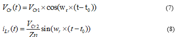
Where Zn is the natural impedance and wr is the resonant frequency of the resonant branch given as:
 As can be seen, the sinusoidal behavior of the resonant branch has no significant effect on the equations of the PWM branch components.
2.2 MOSFET Switch OFF
 Figure 4 MOSEFT OFF, D2 OFF, D1 ON
When the MOSFET switch is OFF, the current iL(t) traverses through diode D1 which is the freewheeling diode, same as in conventional buck converter. The diode D2 turns off and the resonant capacitor Cr begins to discharge in the quasi linear fashion. The resonant inductor current is zero in this mode. The inductor current has a negative slope as shown in the figure. The important waveforms and associated equations for this mode are:
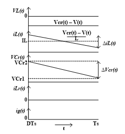 Figure 5 Waveforms in Mode II
![]() As can be seen, the resonant capacitor Cr is quasi linearly discharged from level Vcr2 to Vcr1. The average voltage across Cr will be shown to be equal to difference of input and output voltages. Also note that the inductor Volt-Sec balance equation for mode II is different from conventional buck converter and therein lays the advantage of present topology as will be shown later.
As can be seen, the resonant capacitor Cr is quasi linearly discharged from level Vcr2 to Vcr1. The average voltage across Cr will be shown to be equal to difference of input and output voltages. Also note that the inductor Volt-Sec balance equation for mode II is different from conventional buck converter and therein lays the advantage of present topology as will be shown later.
2.3 DC Gain Characteristics
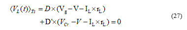
The dc gain of hybrid switching buck converter can be derived by applying principle of volt-sec balance on main and resonant inductors as well as principle of charge balance on main and resonant capacitors [4].
For main filter inductor L:
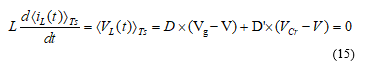 Where D is the main switch duty cycle and D’=1-D. Also we have assumed steady state so the time varying quantities are replaced by their dc values. Solving Eq. (2.14) yields:
![]() Applying Volt-sec balance on resonant inductor Lr yields:
Applying Volt-sec balance on resonant inductor Lr yields:
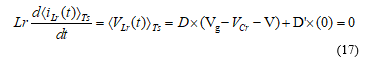 After simplification we get:
![]() Thus the average voltage across resonant capacitor is equal to the difference of input and output voltages. After substituting Eq. (2.17) into Eq. (2.15), we get the desired dc gain as:
Thus the average voltage across resonant capacitor is equal to the difference of input and output voltages. After substituting Eq. (2.17) into Eq. (2.15), we get the desired dc gain as:
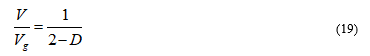 The dc gain is very different from conventional buck converter and (19) suggests that there is a lower limit on the output voltage. For duty ration D=0, we get V = Vg/2. However, in the next section it is shown that this is not the case as main inductor dc resistance reduces the dc gain ratio and thus the converter can traverse almost all the range of output voltage.
Next the principle of capacitor charge balance is applied to main filter capacitor as well as resonant capacitor. For capacitor C, we get:
 After simplification we get:
 Applying Charge balance on resonant capacitor Cr, we get:
 This results into:
 Finally we get relationship between average inductor current and load resistance as follows:
![]() we can also calculate the average value of input current which is the same as main MOSFET average current as follows:
we can also calculate the average value of input current which is the same as main MOSFET average current as follows:
![]() After substituting Eq. (2.22) we get:
After substituting Eq. (2.22) we get:
![]() A summary of DC characteristics of conventional buck converter and hybrid switching buck converter is presented in a tabular form.
A summary of DC characteristics of conventional buck converter and hybrid switching buck converter is presented in a tabular form.
Table 1 DC Characteristics Comparison
| DC Characteristic | Conventional Buck Converter | Hybrid Switching Buck Converter |
| Voltage Gain | ||
| Average Inductor Current | ||
| Average Input Current | ||
| Average Switch Voltage | ||
| Main Inductor ripple ∆iL | ||
| VD1 |
From the above table, following advantages of Hybrid Switching Buck converter can be summarized:
- The inductor current ripple is reduced. This implies that for the same switching frequency, hybrid switching buck converter requires smaller main power inductor. This advantage is achieved without increasing switching frequency.
- Both MOSFET and freewheeling diode voltage ratings are reduced. Low voltage switches with better switching features can be used.
2.4 DC Gain with Inductor DC Resistance
Finally, we derive the DC gain including main inductor dc resistance. For reference, the circuit is produced here including inductor dc resistance:
Figure 6 Hybrid Buck Converter including inductor resistance
Only the Volt-Sec balance equation of main inductor is changed and is given below:
 After simplification we obtain:
![]() Replacing the value of VCr from (18) and simplifying:
Replacing the value of VCr from (18) and simplifying:
![]() We replace value of IL from (24) and simplify to get final equation:
We replace value of IL from (24) and simplify to get final equation:
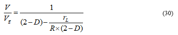 This equation shows the effect of inductor dc resistance rL on DC gain. The DC gain is reduced and thus the converter is able to traverse wider range of output voltage.
3. Small Signal Modeling of HSBC
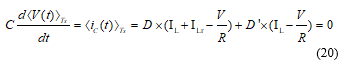
In this section we derive small signal transfer function of hybrid switching buck converter. We can write the large signal equations for the main filter inductor and capacitor using the approach in [4]. The averaged equation for inductor L is given below:
 Where <x(t)>Ts denotes the average of x(t) over switching period Ts. We can perturb and linearize this non linear averaged equation by replacing time varying quantities with their steady state values perturbed in small quantities as shown next:
|
|
|
|
 Where represents the small signal perturbation in steady state value of variable .After replacing in (31), we get following equation:
 After simplification, we ignore dc and higher order terms and arrives on following small signal equation for inductor L:
 Similarly, the non linear averaged equation can be written for the output capacitor C:
 After perturbing and linearizing steps as shown for the inductor, we obtain following small signal equation for capacitor C:
 Applying the similar procedure for the input current ig(t), we have:
![]() After perturbation and simplification we obtain following equation:
After perturbation and simplification we obtain following equation:
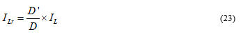
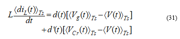
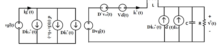
![]() The (33), (36) and (38) represent the small signal model of the hybrid switching buck converter. We can combine these equations to produce the equivalent small signal model of hybrid switching buck converter.
The (33), (36) and (38) represent the small signal model of the hybrid switching buck converter. We can combine these equations to produce the equivalent small signal model of hybrid switching buck converter.
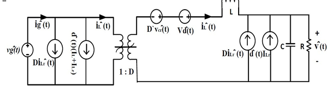
As can be observed, the small signal ac model of the hybrid switching buck converter is similar to the conventional buck converter with the inclusion of additional voltage and current sources due to the presence of resonant capacitor and inductor. However, this circuit can be solved in the manner similar to the conventional buck converter to obtain desired transfer function such as control to output transfer function [4], [5].
On the primary side of the DC transformer, two additional current sources are present. One current source is due to the effect of the change in resonant inductor current. This is because the resonant inductor current is drawn from the input port of the converter. Any change in this resonant current will be reflected in the input current ig(t). The other two sources combined as one represent the effect of change in control variable i.e. duty cycle d(t). The DC values of both the inductor current and resonant current are responsible for this effect. In case of a conventional buck converter, only DC value of inductor current is present here but in case of HSBC both the main power inductor and resonant inductor are charged by the input port and thus both values are present.
As can be observed on the secondary side, there are two voltage sources as compared to the one in case of a conventional buck converter. Moreover, the voltage source consisting of Vg in conventional buck converter is now replaced with one consisting of output voltage V. This can be attributed to the fact that the HSBC applies different volt-sec to the main power inductor as compared to the conventional buck converter. During the time when the MOSFET switch in OFF, the conventional buck converter applies minus V times the off time interval (-V*D’Ts), where HSBC applies Vcr – V time the off time interval ((Vcr-V)*D’Ts). This difference is reflected in the form of change in voltage source on the secondary side of the transformer.
An additional voltage source is due to the effect of change is resonant capacitor voltage. The resonant capacitor voltage is applied only during the off time interval and hence its small signal component is multiplied by the complement of steady state duty cycle.
One might imagine after looking at small signal equivalent circuits shown above that the HSBC is more difficult to control and that its small signal control to output transfer function will be more complex than a conventional buck converter. However, as will be shown in next sections, the small signal characteristics of HSBC closely mirror those of the conventional buck converter. The control of the HSBC can also be accomplished by the identical computational effort as that of conventional buck converter.
4. Digital Control Implementation
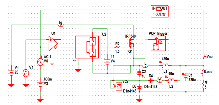
In order to demonstrate the viability of the converter and the potential of simple 8 bit microcontrollers to control this converter, a simple test setup was created in lab around an 8 bit STM microcontroller [5]. The simplified schematic diagram of the implementation is presented below:
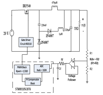 Figure 7 Digital Control Setup
The output of the converter is scaled down by the resistor divider and converted into digital domain by the ADC. The PI compensator block calculates the error and applies compensation to generate the duty cycle for the main switch. The built in PWM block of STM controller is used to generate the duty cycle controlled pulse signal for MOSFET.
The flowchart of the software used to control the converter is shown below:
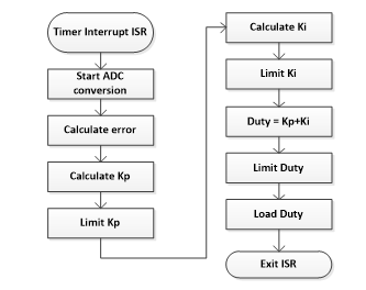 Figure 8 Software Flowchart
It should be noted here that the duty cycle calculated by the PI controller is limited to a certain minimum value to ensure that the duty cycle is always greater than half of resonant period as given by Eq. (2.1). This ensures that the resonant current cycle is completed without any interruption. The concept is illustrated in the next figure.
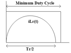 Figure 9 Minimum Duty Cycle
At first glance it would appear that this is negatively restricting duty cycle above a minimum threshold. However, in practical designs, the duty cycle generally oscillates around its designed value in small quantities and very rarely traverses the entire range of its possible values. So, if the converter is designed such that the half resonant period is some small fraction of the duty cycle, say five percent, then this restriction can be met without much problem. In practical setup used for this converter in the lab, the half of resonant period was about five percent of duty cycle and converter operated without problem.
5. Simulation and Practical Results
|
|
The converter is simulated in SIMPLIS simulation software. The screenshot of the SIMPLIS simulation is shown in figure 12.This software provides the ability to simulate the circuit in its steady state form directly, without having to perform lengthy and time consuming transient analysis. This feature of the software is called Periodic Operating Point (POP) analysis.
Moreover, the ac analysis of this converter circuit can be performed in time domain without having to derive equivalent frequency domain models, thereby simulating a real life network analyzer in software [6].
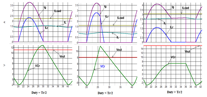
The circuit is simulated for three different values of MOSFET duty cycle, 30%, 50% and 80%. The results of important circuit parameters for these three duty cycles are presented in figure 13.
As we can see from figure 13, the ILr becomes zero in case of duty cycle being greater than or equal to the half of resonant period. In case duty cycle is less than Tr/2, then the diode D4 will be hard switched and incurs switching losses. Therefore, the converter should be designed such that the duty cycle is limited to the values above the Tr/2.The behavior of the resonant capacitor voltage swing should also be considered here. The case in which duty cycle is less than half of resonant period, the voltage Vcr charges sinusoidally up to the point of switch transition and then discharges linearly. The behavior is consistent with the theory of hybrid switching conversion i.e. resonant charging and linear discharging. Also the case in which duty cycle is greater than half the resonant period, the voltage Vcr rises sinusoidally until the current ILr is flowing. When the current ILr tries to become negative, the diode D2 blocks the flow and the current can flow no further. This results in voltage Vcr becoming constant. This, of course, doesn’t affects the converter behavior.
It can be seen that the output voltage can traverse greater range than predicted by the DC gain of (19). This is because of the fact that the simulation software includes the parasitic elements such as MOSFET on resistance and diode forward voltage drops. Such parasitic, like the dc resistance of main power inductor, work to reduce the DC gain predicted by (19), thereby allowing the converter to traverse greater output voltage range.
|
|
It was predicted in the previous section that the small signal characteristics of HSBC are very much identical to those of conventional buck converter. In this section, we present the small signal control to output transfer function characteristics simulated in SIMPLIS software. This software has the capability to simulate the circuit in time domain, thereby emulating the behavior of a network analyzer. The bode plots of the simulation are shown next:
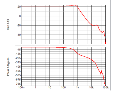 Figure 12 HSBC Bode plot
As we can clearly see, the converter exhibits almost same gain roll off as that of a conventional buck converter [4], [5]. The gain cross over frequency for the simulated circuit comes out to be 2.73 KHz. This shows that HSBC is a stable open loop converter which can be controlled easily using simple control structures.
In order to demonstrate the viability of the converter, a simple prototype was built on breadboard in lab. The setup was arranged according to the figure 9. The following table shows the parameters of this setup:
Table 2 Setup Parameters
| Parameter | Value |
| Input Voltage Vg | 20 V |
| Output Voltage Vout | 10 V |
| Load Resistance | 33 Ω |
| L | 470µH |
| C | 220µF |
| Lr | 1 µH |
| Cr | 220nF |
| MOSFET | IRF540N |
| Diodes | IN4007 |
| Switching Frequency | 50 KHz |
The breadboard setup in the lab and the results are presented next:
The breadboard setup consists of a simple assembly of HSBC. The converter is essentially derived from a buck converter presented in [5]. The STM discovery board is used to control the converter using a PI controller. The results of the converter operation are presented next.
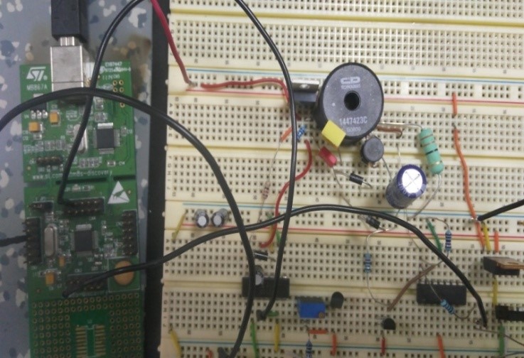 Figure 13 Breadboard Setup
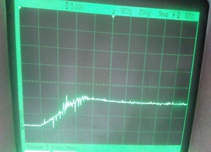 Figure 14 Voltage Startup Response
The output voltage startup response presents good picture with reasonable rise time for an 8 bit controller. The response time should be adequate for general power conversion applications not requiring stringent response constraints.
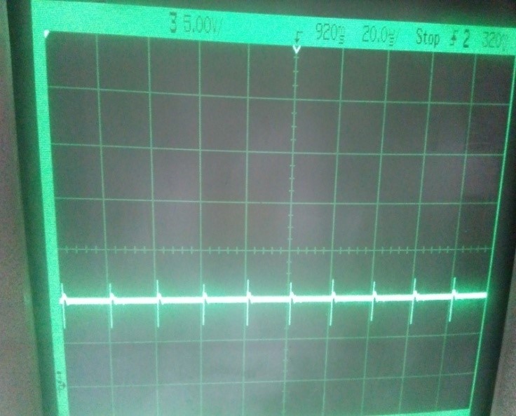 Figure 15 Steady State Output Voltage
As can be observed, over the period of various switching cycles, the converter exhibits no limit cycle oscillations. Therefore, this converter can be controlled using a simple PI controller. The output voltage can be regulated within reasonable bounds depending on the applications.
6. Potential Applications
The hybrid switching buck converter presented in this paper belongs to a new class of converters and as such is unfamiliar to practicing engineers. Although at first glance it may appear that the part count for this converter is increased when compared to a conventional buck converter, however, the advantages presented by this converter can overcome such issues.
First, if the converter is designed carefully, the diode D2 in series with resonant inductor is soft switched thereby avoiding switching losses. Second, the most significant portion of the PCB is taken up by magnetic in a dc-dc converter. For example, in an MPPT solar battery charger dc-dc converter, the inductor core is the largest component in the power converter. The hybrid switching converter provides the reduction in the size of main power inductor and is therefore suitable for such applications.
Another area of potential application can be the converters that require reduction in size due to space constraints, such as integrated dc-dc converters for military and space applications. Such converters can benefit from this type of hybrid switching buck converter.
7. Conclusion
In this paper, a hybrid switching buck converter was presented. The concept of hybrid switching was introduced. The DC conversion ratio of this HSBC was derived and its dc characteristics were compared to conventional switching buck converter. It was shown that HSBC results in reduced magnetic size without increasing switching frequency of associated switching losses. The small signal analysis was performed on this HSBC and the result was shown to be familiar to the conventional buck converter. The simulation and practical results of digital control using 8 bit microcontroller were presented. The potential application areas of this HSBC were discussed.
CONFLICT OF INTEREST
The author declares no conflict of interest.
- S. Cuk, “Step-down converter having a resonant inductor, a resonant capacitor and a hybrid transformer,” U.S. Patent 7915874, Mar. 2011.
- S. Cuk, Z. Zhang, “Voltage step-up switching DC-to-DC converter field of the invention,” U.S. Patent 7778046, Aug. 2010.
- S. Cuk, “Bridgeless Power Factor Correction,” U.S. Patent 2010/0259240, Oct. 2010.
- Erickson, R.W., Maksimovic, D., “Fundamentals of Power Electronics”, 2nd Edition, Kluwer Academic Publishers, 2000.
- Abbasi, Muhammad Umar, “Digital Control of a Buck Converter using an 8 Bit STM Mircocontroller”, International Journal of Scientific & Technology Research Volume 6, Issue 04, April 2017, ISSBN 2277-8616
- SIMPLIS Technologies, www.simplistechnologies.com