Design for Smaller, Lighter and Faster ICT Products: Technical Expertise, Infrastructures and Processes

Adv. Sci. Technol. Eng. Syst. J. 2(3), 1114–1128 (2017);
 DOI: 10.25046/aj0203141
For the design of Information and Communications Technology (ICT) related products, basic level of technical expertise and simple development tools were enough in the early 1980s. As time goes by, new generation products designed by engineers are always expected to be smaller, lighter and faster, due to the increasing global competition and the application of hardware and software in every area of our lives. In order to be able to respond to these needs, engineers have always had to produce new technologies and solutions. In this sense, hardware related technologies have been growing much faster such as System on Chips (SoC), displays, batteries and other materials used in the ICT products. Designers have been diversifying software development processes and tools remarkably for new applications and constantly developing new communication standards. In this article, all the main design phases are presented starting from the system design to the product validation and test. As can be seen from the relevant sections, in order to design an ICT product, very deep technical expertise, expensive development and verification infrastructures are needed in the relevant fields.
1. Introduction
Before the 1980s, in the design process of Information and Communication Technology (ICT) products, it was sufficient to have technical expertise at the basic level such as entry-level material knowledge, basic skills in using measurement equipment, and the ability to use simple compilers in related fields. In those years, functionality was the main concern for the product design. Furthermore, the development processes and infrastructures were much simpler than today. In the modern era, due to the advents in technology, the emergence of new composite materials, the introduction of effective production methods and the rise and on-going diversification of consumer expectations, product design process is getting more complex. In order to meet new product development requirements, a multidisciplinary approach is required to synthesize respective knowledge from various disciplines, such as anthropology, sociology, physics, chemistry, environment, etc.. In the rise of today’s consumer culture, functional satisfaction is no longer a mere reason of purchasing goods and services, while social factors substantially affect consumer decisions. Especially for mobile and wearable ICT products, the owned products are tools through which consumers express their identities. Thus, besides the proper functionality of the product, different factors, such as emotional response of the customers should be taken into account in the product design. Therefore, today’s development processes are becoming too complex and multifaceted.
The first commercial microprocessor was Intel 4004 (4-bit), which was intended for use for use in a calculator in 1971 [2]. Today, multi-core processors with high processing power are required in the design of broadband wired or wireless products or high-capacity IP (Internet Protocol) switching devices. These processors include dedicated coprocessors, special data transfer paths and data processing units, along with a large number of ARM (Advanced RISC-Reduced Instruction Set Computing-Machine) and DSP (Digital Signal Processor) processor cores running at gigahertz speeds [3]. In order to meet wide range of the required features, it is necessary to develop high performance software spread across tens of thousands of source files and, composed of millions of lines, which is designed to exploit the potential of the available hardware resources [4]. On the other hand, the hardware provides multi-core CPUs capable of performing hundreds of billions of operations per second and very high-speed and high-capacity data transmission interfaces. In addition, for the design of an ICT product, technical expertise and dedicated infrastructure is required related to mechanical design, thermal analysis, electromagnetic compatibility, product integrity and reliability, product testing and verification. As a result, the complex technological structure of ICT products entails the use of various advanced engineering skills in the design process.Until mid 1970s, the design and manufacturing processes of ICT products were mostly based on nonautomated or semi-automated processes, where technical hand-skill of the operator usually plays a crucial role. PCB (Printed Circuit Board) design and production were made by hand work, with Letraset and paper [1]. The use of the computer in the design process of ICT products was a revolution. Computer-aided design not only accelerated the design and manufacturing processes, but also resulted in a significant reduction in the related human errors. Moreover, the decrease in the duration of the design allows the production of more complex ICT products. The automation of the manufacturing of ICT products greatly increased the manufacturing volume and reduced the cost of the products that could provide the functionality never achieved before.
In this article, various technical expertise, infrastructure and processes necessary to design an ICT product will be described. These technical expertises are related to system design, hardware design, mechanical design and software design, verification and production.
After a brief and formal definition of system design given in Section 2, issues in today’s hardware design is discussed in details in Section 3. In this section, PCB design, signal and power integrity, recent developments in IC (Integrated Circuit) technologies, developments in manufacturing technologies, System on Chip (SoC) technologies, recent developments in RF (Radio Frequency) design and EMC/EMI, and concerns related to energy efficiency are considered. In this section, the requirements of a specific hardware design in today’s technology are considered as an example.
Section 4 is concerned with mechanical design and discusses design considerations in the choice of materials to meet the requirements of the used process.
Section 5 discusses issues in software design. In this section, the development steps and troubles from the past to the present are given, followed by the related development processes, which are formed because of these progresses. In this section, trends emerged in the field of software development, especially in virtualization technologies, open source code development and effective use of frameworks are considered in order to create cost effective short-term software development. In addition, virtualization and IoT (Internet of Things) software emerged in this field are discussed. In Section 6, software validation tests and test methodologies are considered. In Section 7, the state-of-the-art ICT production processes are described and discussed. Finally, in Section 8, a practical implementation for a cutting edge ICT product design is described.
2. Design for Requirements: System Design
System engineering manages the product development process by taking into consideration the technical requirements, time and cost elements of the product design, production, delivery and maintenance activities [5]. System engineers may suggest either a new product on a new product or adding a new feature to an existing product, based on the feasibility study. Prior to a detailed system design, the general system-level design needs to be prepared by the system engineers. After performing a detailed study of product description, the functional behaviour and the basic system architecture are developed. This is the most critical step in the design of complex products. The ability to meet the additional requirements for the designed system depends on the flexibility and extensibility of the system design. For a system engineer, expertise and skills in all areas described in this paper are required in order to achieve the necessary engineering activities.
3. Design for Software Platform: Hardware Design
Hardware design consists of establishing system and/or subsystem hardware and mechanical infrastructure in order to achieve defined system, software and platform requirements. These requirements are concerned with the platform, mechanical dimensions, power consumption and environmental conditions, such as high/low temperature, humidity, shock, vibration, radiation, air pressure, Electromagnetic Compatibility (EMC) and Electromagnetic Interference (EMI).
In this Section, first PCB design with signal and power integrity issues will be introduced. After that, the evolution of hardware IC design and developments in manufacturing techniques will be explained. Later, SoC IC concept; application specific and high capacity ICs with multiple functions and interfaces will be pointed out. On the last part, 3D(3 Dimension) IC design technique for smaller and less power consuming ICs, developments in RF design, EMI/EMC and energy efficiency subjects will be covered.
3.1. PCBs (Printed Circuit Boards)
The first PCBs were used as early as 1900’s. In those years, various materials like Bakelite and Masonite, plain old thin wooden pieces were used as PCB materials [6]. These PCB materials were drilled into the holes and the brass wires were riveting on the material. Over the following years, circuit sizes were reduced with the use of double-sided and multilayer PCBs and hot air soldering methods.
In the 1980s, surface mount components became the preferred option rather than through-hole components. In the 1990s and 2000s, the complexity of modern circuit boards increased and “micro-via” technology emerged in PCB manufacturing. In those years, the use of 5-6 mils of trace and space on PCBs was getting more widespread. On the other hand, Flex and Rigid-Flex PCBs have become an economical option and widely used. Today, ELIC (Every Layer Interconnect) technology allows for dynamic connection between any two layers within the circuit layout.
Nowadays the number of layers in a typical high-density PCB has increased up to 40. There are more than 350 kinds of dielectric materials in aerospace, communications, high-speed digital design, power, and wearable device areas. The operating frequency for epoxy / glass (FR4) material has been increased to 40GHz. In recent years, flex and rigid-flex cards have gained popularity. Since rigid-flex cards require fewer connections, they are more reliable and their long-term maintenance cost is reduced.
Printed Circuit Design was made manually before the introduction of Computer Aided Design (CAD) tools. Placement of the components is done on transparent paper with ICs plotted as templates. Using this paper, a film that corresponds to the circuit layout is prepared and by the use of dry transfer technique, PCB is produced. PCB design is finalized by adding copper lines formed using Letraset papers.
Today there are several advanced CAD tools for the hardware design development. These tools enable multi-layer PCB design with high-speed signals and allows the diagnosis of layout problems related to built-in signal integrity, power integrity, cross talk, reflection add-on’s before PCB production. Using 3D modelling features of these tools, mechanical mismatches can be detected on 3D PCB layout view. With the help of these tools, multi-layer, densely populated PCB design including high-speed data paths with low latency providing hundred billions per second processing power can be accomplished [7].
Figure 1 shows the layout of the baseband card of a 4G base station. On this card, there are both high-speed data paths (>50 Gbps) and high-speed transmission lines for inter-card communication (>10 Gbps). The design of the PCB enables the reference clock signals (312.5 MHz, 156.25 MHz and 122.88 MHz) to have very low jitter (4 ps RMS) and very small 50 ps rise/fall time.
 Figure 1 PCB layout for a 4G baseband card.
3.2. Solving Transmission Issues for High Speed Digital Design: Signal & Power Integrity
Signal Integrity deals primarily with the signal transmission performance within an electronic product. This issue is due to the electromagnetic behaviour of the system and the tools to study the related effects remain more or less the same since the beginning of electronic transmission. First transatlantic telegraph cable was exposed to serious signal integrity problems, and this led to invention of the mathematical tools for signal integrity analysis, such as telegraph equations, which we still use today [8].
Typical ideal and real waveforms of a signal are shown in Figure 2.
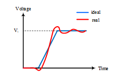 Figure 2 Ideal and real waveforms at the receiving gate.
On PCBs, when propagation delay of a signal approaches signal transition times (rise/fall time) and the system speeds exceed a few tens of megahertz, signal integrity analysis becomes a necessity. Today signal speeds reach several GHz.
Since 1990’s, the requirements for signal integrity analysis are getting more and more important. Initially, PCB trace speeds have become an important issue in the PCB design. Designers approached this problem by considering analog characteristics of digital data paths. The main objective of signal integrity study is to ensure reliable transmission of digital signals between transmitter and receiver. While initially the main focus in signal integrity study was the connection between transmitter and receiver, in modern designs, signal integrity models are used in the design of transmitters, receivers and every part in between.
By the years of 2000s, power supply for digital circuits has become a big problem and a need for Power Integrity (PI) analysis has emerged. Signal integrity (SI) analysis shows signal’s behaviour through PCB traces, conductors and passive elements. However, PI analysis examines power distribution lines by evaluating power plane impedance and decoupling capacitors. While PI is related to the system reliability analysis, its main goal is to ensure that drivers and receiver have enough current to send and receive 1’s and 0’s [9].
In the early phases of electronic circuit industry, available ICs came with one power and one ground pin. A bypass or decoupling capacitor between the power rail and the ground pin was more than enough to filter out the noise. Today, a complex Ball Grid Array (BGA) features hundreds of power and ground pins and more than 10 different voltages under 1V. These complex ICs typically draw currents of tens of amperes. In order to supply clean and noiseless power at these levels, a large capacitor network is required. The effective design of this capacitive network requires the accurate analysis of the propagation of energy in a power distribution network, which includes capacitors, vias and power/ground planes. For instance, , since 1990s the operating voltages drops from 5V to sub 1V’s, where operating currents rises from 1A to several 10A’s. These show that power consumption rises from 5W to several 10W’s and impedance target drops from 500mΩ to1mΩ.
Today, EMC and Signal Integrity (SI) are the most important issues in electronic product design, which should be considered through all the design process. The main reason is the high data bandwidth demand of new generation high performance products and servers, which operate over hundreds of Gbps. EMC and SI Technologies on PCB and IC packages are one of the bottlenecks at these bandwidth requirements.
In Figure 3, the variation of signal rates used in serial links in the last 40 years is shown.
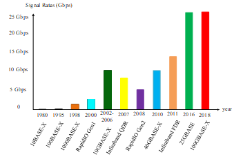 Figure 3 Signal rates of serial links in the last 40 years.
As seen in this figure, signal rates that were around 10 Mbps for 10 Base-X Ethernet in 1980, have reached 25 Gbps today. An interesting feature in this graph is the decrease in signal rates, which appear in years 2007 and 2008 [10]. In these years, implementation difficulties of 10 Gbps per line on long backplanes due to signal integrity issues led way to interconnect standards consist of multiple port high-speed serial lines such as RapidIO or Infiniband QDR. In 2007, Infiniband QDR drops line rate to 8 Gbps, however supports operation on four parallel lines to achieve 32 Gbps data throughput. In 2008, Serial Rapid IO standard defines the maximum line rate as 5 Gbps and supports 2, 8 and 16 parallel lines, which in turn supports total throughput of 10, 40 and 80 Gbps respectively.
One possible approach to increase data rates is to increase the Non-Return-to-Zero (NRZ) data rate with very high-speed serial links. Another possible way is to encode the data using PAM4 (Pulse Amplitude Modulation). Using PAM4 modulation, it is theoretically possible to reach a collective data transfer rate of 800 Gbps.
Nowadays, for PAM-4 coding, 13 GHz clock frequency is used and 400 Gbps Ethernet speed is reached with 8 lines, each featuring 53 Gbps speed [11].
As mentioned above, the ultimate goal is still smaller, lighter and faster products. In order to achieve these goals, additional issues such as the implementation of appropriate inter-system connection interfaces should be taken into account. In order to meet the design requirements, robust, miniature and high-speed connectivity solutions should be considered.
3.3. Progresses on Integrated Circuit and Manufacturing Technologies
The fastest change in the semiconductor technology era emerges in the field of processor and memory oriented semiconductor manufacturing. The key drive factors in this evolution are higher speed (executed commands per second, data transfer rate) and higher capacity (memory, number and different types of interfaces). Transistor size in IC’s reaches from several micrometers to tens of nanometers. The prediction of Gordon Moore, one of Intel’s co-founders, about transistor number in a dense integrated circuit will double every two year in 1965, proved to be right in the following 50 years as can be seen in below Figure 4 [12].
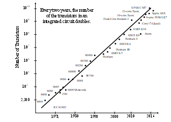 Figure 4 Number of transistors for CPUs and Moore law.
Due to the high integration capability, programmable semiconductors for different features in the same package can be developed for digital circuits, interfaces, power electronics, RF (Radio Frequency) and analog circuits as well as processors. Every new integrated circuit has more rule set and documentation for usage. Design, manufacturing and test processes become more and more complex and need different methods and tools than the previous ICs.
In recent years, performance and success metrics in integrated circuit design and manufacturing has changed dramatically. Up today, the main success metric for personal computer ICs is clock speed. Therefore, the manufacturing technology has developed according to these criteria. Nowadays, form-factor, cost and power consumption are the critical driving factors, especially in mobile market; that in turn has increased the importance of on-chip integration of functional hardware (e.g. power management, computing, audio/video, graphics and radio). In order to integrate these hardware on-chip, specifically designed for purpose design and simulation techniques are used. Today, there are around 20 fabs that can manufacture analog and basic digital ICs with 130nm ~ 28 nm process where there are only 5 fabs which can use 14/10nm process to manufacture market dominator SoCs [13].
The need in the present decade drives technology markets to use more and more integration such as mobile communication, data centers, automotive and IoT platforms. This demand has increased the importance of lower nanometer process and more complex manufacturing technologies. 7 nm processes is expected to be realized within the next two years, where studies and early trials continue for 5 nm [14]. As a result, more analog and digital functional block will be integrated within a single chip. Analog functional blocks will be manufactured with 14 nm process and very low power analog/RF circuits targeting IoT platforms can be designed. FinFET (Fin Field-Effect Transistor) technology may be one of the viable methods to achieve this goal.
The distinctive feature of the FinFET is that the conducting channel is wrapped by a slender semiconductor “fin” that forms the body of the device and the fin thickness determines the effective channel length of the device. FinFET technology will be the basic infrastructure for the complex semiconductors produced within next decade. Because of its features like the ability to be fabricated with its channel along different orientations in a single die due to its nonplanar structure, the reduction of “Short Channel Effect according to its fin thickness and fin length, ability to control its threshold voltage with multiple voltage sources and reduction of off-state current. For example, a mobile chipset produced with 14 nm FinFET technology in August 2016 is performing % 30 faster, increased core speed by % 20 and consumes % 35 less power compared to its predecessor [15].
3D IC comes forward as an alternative to improve manufacturing technology and managing processes under 14 nm. 3D ICs are manufactured by placing silicon layers vertically on top of each other and connecting layers with TSVs (Through-silicon vias). Using this technology, a cost and performance effective development can be accomplished. $16 billion investment is forecast to build a foundry for a more advanced technology level of 7 nm process node [16]. 3D IC design is discussed in detail in the section 3.6 for size reduction and low power consumption purposes.
3.4. Processors: CPU, GPU, NPU, APU, PPU and TPU
CPU (Central Processing Unit) is the central processing unit of computers. After the invention of transistor, Intel 4004 CPU with 2300 transistors was produced in 1971 using a 10 µm technology operating at 740 kHz. Today, processors can be manufactured with 14 nm technology and contain 10 billion transistors. These processors are capable of running at 4.2 GHz speeds and support many types of instruction sets. General-purpose processors perform general purpose operations and are used in many areas, especially in personal computers and [17].
In GPU (Graphical Processing Unit) processors, it is important to have parallel command processing capabilities, as well as sequential processing capabilities that conventional CPUs have. This feature is also used for accelerating computation in areas such as 3D rendering in computer games, advanced scientific research, oil and gas exploration and self-controlled driving technology [18].
In terms of architecture, general-purpose processors can be made up of several CPU cores and can do several jobs simultaneously. Similarly, GPU processors have hundreds of cores to process parallel jobs efficiently. Today, Multi-GPU processors with many GPU processors are produced [19].
A NPU (Network Processing Unit) is a dedicated processor specially designed to perform network related functions. While these units are often intended to be used in embedded systems, they are also employed in the personal computers. For example, Mellanox’s Indigo NPS-400 unit has an internal processor unit, which provide all services including traffic management at 400 Gbps capacity. This processor has development support in C programming language [20].
Large processor vendors such as Intel and AMD (Advanced Micro Devices) have developed APU (Accelerated Processing Unit) technology by combining the superior features of CPUs and GPUs. APU processors are used in areas where power consumption and performance are important. For example, a large GPU manufacturer Nvidia has collaborated with the ARM Company, to produce the APU named Tegra, and has entered the mobile and smartphone markets [21].
A PPU (Physics Processing Unit) is an interface, which has been developed for processing physics rules in graphics processing. These processors compute special operations such as the effect of gravity and the effects of collision of objects in accordance with the laws of physics. It was originally developed by Ageia in 2006. However, after merging with Nvidia, it is developed continuously as a middleware running on GPUs under the name PhysX [22].
A TPU (Tensor Processing Unit) is developed by Google for TensorFlow open source library. It is application-specific ASIC technology specially developed for machine learning. These units are widely used in the data centers of Google. An important asset of these units is reduced computational accuracy compared to GPUs. However, since fewer transistors are used in these units, they offer better performance than their counter parts in terms of unit power consumption [23].
3.5. Design for High Capacity: SoC (System on Chips)
In the ICT products developed today, processors, which include several different functional blocks, are used for high capacity and special function needs that cannot be met with generic processors on the market. In these processors, there are several CPU cores, general-purpose DSP cores and application-specific co-processors, which provide low latency required in applications such as error coding/decoding and Fast Fourier Transform (FFT) algorithms. These processors provides performance, easy development cycle, flexibility and product cost advantages. Today, programmable SoC, FPGA based SoC and RF specific SoCs are used for different applications.
Today, SoC manufacturers are purchasing the IP Core license from ARM to integrate it into the chip design. In this way, fabless companies can develop designed, tested and production ready processor cores. The new chips designed by these companies are produced in semiconductor fabrication plants (fabs) to meet high performance and low-cost requirements [24].
Figure 5 shows functional block diagram of a general SoC used in the design of ICT products.
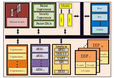 Figure 5 Functional block diagram of a SoC.
- PSoC (Programmable System on Chip)
A cost effective solution to general purpose SoC ICs are programmable SoCs, which includes only specific functional blocks and interfaces required in the designed system. Using this architecture, unused functions and interfaces are not integrated into the specifically designed ICs and this provides the main advantages of ASIC (Application Specific Integrated Circuit), such as performance, form-factor and product cost. The availability of the optimized use design of these functional blocks reduces design time and eliminates nonrecurring engineering cost of programmable SoCs. The flexibility of this architecture enables adding or removal of functional blocks in a very short time. Currently, these PSoCs can provide low capacity microcontroller, memory and interfaces and therefore they are being used for products and solutions targeting IOT platforms [25]. Cypress announced that an IOT solution using PSoC 6 series will be provided soon.
3.5.2. FPGA Based SoC (System on Chip)
To provide an alternative to general purpose processors used in product design, FPGA firms developed “soft” processors that can be put into standard FPGA components as object or source code. “Microblaze” and “Picoblaze” processors are good examples for this approach. The next step is placing “hard” “Power PC” processor core into “Virtex” FPGA. The latest FPGA family ZYNQ includes 2 ARM cores as standard product. ZYNQ Ultra scale+ SoCs are produced with 6 ARM core and 1 GPU (Graphic Processing Unit) core [26].
Central Processing Units (CPU) work sequential by design, increasing their performance can only be accomplished by increasing operating frequency or number of CPU cores. FPGA based processors have the advantage of parallel processing architecture, low latency and gigabit high-speed interfaces.
3.5.3. RF SoC (System on Chip)
In the future of the communication, transport, energy and automotive sectors as well as vertical IOT market, integrated circuits produced with low nanometer technologies are expected to be dominant. AMS (Analog-Mixed Signal) technologies and nm based analog block manufacturing processes used during production of these ICs are the main differentiating factor. Because of increased device model complexity of FinFET, complex layout effects impacting design specs, increased parasitic complexity, low-voltage driving intensive noise analysis issues during transition into nanometer production process reveals long and lots of simulation work and huge net lists. Lacking of fast, nm-accurate mixed signal verification limits design and manufacturing success, which leads to 50% first silicon failures. Research continues to integrate analog, digital and RF technologies to provide ultra-low power requirement of IOT applications. Main focus is developing new mixed-signal circuit architecture. In addition, the need and usage of RF MEMS (Micro Electro Mechanical Systems) in satellite communications, radar systems, and adjustable antennas increases.
3.6. IC Design for Size Reduction & Low Power: 3D Integrated Circuits
As mentioned in section 3.3, 3D integrated circuit emerged out as an alternative to improve manufacturing technology. Ever since the combination of analog and digital integration becomes a necessity; 3D ICs, which enables manufacturing of functional blocks with different technologies and rule-sets separately and integrate them in the last stage of the production, offer significant improvements over two-dimensional circuits. Average connections inside 3D ICs are much shorter and interfaces inside the IC can be work faster consuming less power. An application processor designed as 3D IC is reported to have 43% less space, 13% less power and 14% less connection length in average compared to conventional designs [27].
Figure 6 shows 3D IC structure including many different circuits with 3D interconnect.
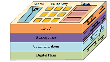 Figure 6 Different circuits on the same die, tied together with different 3D interconnect.
3.7. Batteries
When choosing a battery for a product, there are many criteria to take into account, such as capacity/volume, charging duration, voltage match, polarization/rate capability, weight, and cycle life/shelf life, operating temperature range, safety, toxicity and cost. For instance at the beginning of 1900’s nickel cadmium batteries helped pave the way for modern technology, but because of cadmium’s toxicity, alkaline batteries spread in the market after 1950’s. Alkaline batteries were safer and cheaper but their energy density was not enough to supply high performance devices.
While electronic devices are getting more and more complex, more energy density and form factor are required. Nickel-metal-hydride and lithium-ion, emerged in the early 1990s, provides high energy density. For example, the energy density of lithium-ion is typically twice that of the standard nickel-cadmium. Today, lithium-ion is the fastest growing and most promising battery chemistry [28].
The high cell voltage (3.6V) capacity of li-ion’s allow battery pack designs with only one cell and most of today’s mobile phones run on a single cell. A nickel-based pack would require three 1.2 V cells connected in series. This allowed smart phones to have relatively larger display size and longer lifetime [29]. Lithium-ion batteries suit well to low temperature and warmer environments compared to NiMH cells. Li-ion can operate to a temperature of as low as –40°C that increases the data security at harsh environments.
There are specific cathode types for each application for instance laptops and smartphones use lithium cobalt dioxide (LiCoO2) and electrical vehicles use lithium nickel cobalt aluminium oxide (LiNiCoAlO2). Nearly half of the global cobalt supply is being used by in lithium-ion battery industry. Therefore in order to overcome from the lack of cobalt and achieve better battery performance researchers work on different alternative technologies such as calcium ion batteries, Na-Ion batteries, metal-air based rechargeable batteries and sulphur based rechargeable batteries.
3.8. Sensors
- Magnetic Sensors
Essentially there are two types of magnetic sensor: which measures total magnetic field and magnetic field vector components [30]. There are various ways to sense magnetic fields and there are also many factors such as size, sensitivity, linearity, range, frequency bandwidth, dimensions, cost and power, which affects what sensor is best suited for an application.
Magnetic sensors contributed lots of field in ICT and industry. For instance, computers now have storage disks with very big capacity, higher safety standards have been achieved because of the high reliability of without contact switching in aircrafts [30].
Magnetic sensor application may be listed in four categories as given below.
- Low-Sensitivity Application: Hall Effect sensors are most commonly used ones to detect fields greater than the Earth’s field.
- Medium-Sensitivity Applications: Anisotropic Magneto Resistance sensors have become standard off-the-shelf devices for use in medium-accuracy applications, such as compasses for mobile devices [31].
- High-Sensitivity Applications: Flux-gate sensors are widely used in military industry to detect ferromagnetic objects such as a mine, ship, tank, or aircraft [31].
- Medical/Biological Applications: The SQUID sensors are mainly used in bio magnetic applications, which helped to measure extremely weak magnetic fields generated by the brain [32].
- Accelerometers
An accelerometer measures linear or angular acceleration. There are many types of accelerometers developed and reported in the literature. The vast majority is based on piezo-electric crystals, but they are too big to use in small products. Therefore, engineers developed smaller accelerometers using MEMS (Micro Electromechanical Systems) technology [33].
With their robust sensing with little power consumption, MEMS accelerometers have an important commercial potential [33]. Accelerometers are also used in medical equipment such as prosthetic arms. Another important application field is inertial navigation.
Inertial navigation is a navigation technique, which incorporates accelerometers and gyroscopes to track the position and orientation of an object relative to a known starting point, orientation and velocity [34]. For example, PIGA (Pendulous Integrating Gyroscopic Accelerometer) type of accelerometer is used in inertial navigation systems. PIGA sensors are used in guidance system of missile systems today, such as German Rocket V2 [35].
3.9. Displays
Until the beginning of this century CRT displays, which have low picture quality had been widely used in computers and televisions [36]. In the last 20 years, various display technologies have been developed by researchers. Generally brightness, contrast ratio, resolution, size, number of colours, viewing angle, power consumption, response time and life time are key points when selecting the right display for your application. LCD, LED and OLED displays have been most commonly used in consumer products and with the development of rugged touch displays defence industry has started to use them in many applications. Sun light & night vision readable, glove friendly touch screens are the most popular ones in defence industry. Additionally, helmet mounted wearable displays provides augmented data and reality for the next generation soldiers.
Progress in LCD technology has enabled the development of thin, high definition, large display screens. The development of curved screens has been provided with OLED technology. On the other hand, with the development of LAFi (Luminous Array Film) technology curved super-large screens are possible [37].
There are also other display technology such as DLPs, PDPs, FEDs, and electronic paper (electronic ink) competing for market share [38].
In recent years, considerable attention has been paid to 4K, or 8K TV displays, that makes the viewer feel immersed in the image scene [39]. 3D holography image, bendable flexible display with plasma technologies are also hot topics in this field.
3.10. RF Design for 5G
5G (5th Generation) communication technology and IoT are the main driving applications shaping future RF technologies. 5G technology is being developed as a solution for high data speed, low-latency and low power consumption requirements of Ultra HD, 360 degree video transfer, VR (Virtual Reality), smart home, smart city, autonomous vehicles, M2M (Machine-to-machine) communication applications. All these applications require high bandwidth to answer high data throughput needs. Existing bandwidths of frequency bands used for cellular communication cannot support requirements of 5G, research is being done to use 10 GHz, 28 GHz, 32 GHz, 43 GHz, 46-50 GHz, 56-76 GHz and 81-86 GHz bands [40]. Radio signal on these candidate frequencies is deeply affected by atmospheric fading, rain, buildings, human beings, flora and reflection. To overcome these difficulties in RF design, signal processing studies focus on adaptive beamforming. With adaptive beam forming, high data speeds according to the receiver locations can be achieved [41]. Complex circuit structures are used to solve the problems of adaptive beam forming and massive MIMO (Multiple-Input Multiple-Output) technologies. RF Insertion Loss should be lowered to reduce circuit complexity, dimensions and power consumption, which are usually very costly in microwave frequencies. Zero-IF architecture is used for this purpose. The resulting local oscillator leakage issue in Zero-IF architecture is solved with signal processing techniques in digital domain [42].
From semiconductor technology perspective, GaAs (Gallium Arsenide) is the dominating technology of microwave industry for years. SiGe (Silicon-Germanium) technology has major benefits over GaAs in high-speed applications. SiGe BiCMOS (Bipolar Complementary Metal-Oxide Semiconductor) technology also fulfils high-level integration requirements of beamforming systems [43].
Mechanical design is also an important part of RF IC design. Substrate and antenna should be taken into account in order to minimize the losses in integrated circuit design. Less than 50 GHz, antenna and several passive components can be designed as part of the substrate. Studies on SIW (Substrate Integrated Waveguide) continue to be used in this type IC designs. Antenna elements above 50 GHz are small enough to fit into integrated circuit [44].
3.11. Design for EMC/EMI
EMC and EMI technologies become a critical design criteria due to technological developments [45,46]. When necessary precautions against EMC and EMI are not taken during design process, design time and hardware design, mechanical design and test cost can be much higher. To verify if EMC requirements of the designed system are met, very expensive test infrastructure (anechoic chamber, signal generators with several signal types and output power, spectrum analysers, antenna, etc.) should be established. If required by regulations, these tests should be carried by certificated labs.
Today, the voltages in the circuits are low and the currents are high. For this reason, noise and interference problems in digital circuits are mostly due to magnetic field and inductance. For this reason, engineers should take precautions for the magnetic field instead of the electric field for the products they develop [47].
3.12. Energy Efficiency
Total electric consumption of the world has reached 20567 TWh (Tera Watt hour) in 2015 [48]. ICT sector share is %4.6 of total power consumption [49]. Although the figure is relatively low, studies to reduce electric consumption continue due to environmental concerns and cost. Sector participates in initiatives such as EARTH (Energy Aware Radio and network TecHnologies). In addition, operators with the collaboration of universities and research institutes conduct studies about future network infrastructures to reduce CO2 emission.
Figure 7 shows global energy network infrastructure and energy consumption of user terminals [50].
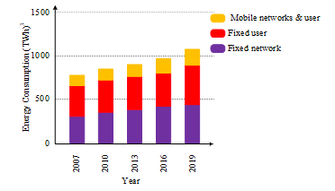 Figure 7 Global energy consumption for network infrastructure and user equipment during operational phase.
The first studies in mobile communication aimed to reduce energy consumption, targeted reducing current draw from battery in order to extend battery life. Advanced RF design techniques like linear and efficient PA (Power Amplifier) design with envelope tracking, adaptive transmit power control, radio aware software management, and development in semiconductor production, extend the battery life of smart phones from 310 minutes to 430 minutes in 5 years [51].
Increasing data requirements of smart phones, laptops and smart TV devices raises energy consumption of mobile communication systems. According to ITU (International Telecommunications Union), energy consumed in the network is %10 of the energy consumed by ICT eco-system and this value is sufficient to illuminate the entire world in 1985 [52].
In mobile communication sector, %80 of the energy is consumed in base stations [53]. Most of this energy is spent for cooling equipment, transmission losses, power amplifiers, transmitter/receiver devices, baseband processing and AC/DC and DC/DC converters.
Base stations do not operate at maximum capacity most of the day. Reducing power consumed at this low traffic intervals, reduces CO2 emission and operator costs dramatically. For this purpose, antenna muting, small cell usage and power-save mode implementation on radios are widely used.
Passive cooling design, their ability to provide service at network edge and low RF power of Small Cell devices helps to reduce operational costs. Small Cell usage improves battery life and coverage area for the users as it helps operators by optimizing energy consumption and easy-to-deploy characteristics in crowded areas.
Figure 8 shows power consumption in cellular networks [54].
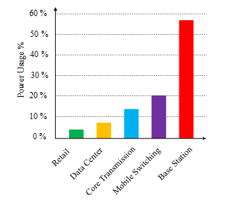 Figure 8 Power consumption in cellular networks.
Macro base stations are becoming more efficient over time. Thanks to improvements in active RF component design, it was possible to use RRH (Remote Radio Head) units. RRH units contribute to energy efficiency because they are designed with passive cooling and are close to the antenna, reducing RF transmission losses. For example, because of the 3 dB reduction in transmission losses to the antenna using RRH, the output power of the power amplifier is reduced by half.
As the use of massive MIMO and adaptive beam forming technologies in base stations, the power used per transmitted bit is reduced. In these technologies, passive cooling is possible because of the use of many small amplifiers in the base station and because the amplifiers are spread over a large area. On the other hand, the beam gains generated by a large number of antennas are significantly increased. This means that less power is consumed from each power amplifier. In addition, as the capacity of the base stations increases, the total amount of energy consumed by the network decreases.
Use of small cell base stations, massive MIMO and adaptive beam forming technologies and use of RRH devices equipped with technologies such as envelope tracking and Doherty design GaN amplifier will enable lower power consumption.
3.13. An Example: LTE-Advanced Baseband Hardware Design
For today’s advanced technology product design, the LTE-Advanced (Long Term Evolution) Baseband unit is an example. This unit has various peripheral cards such as baseband cards, backplane, redundant control card, fan card and power card. There are various high speed signals (Ethernet, Serial Rapid I/O, SGMII Ethernet) in the backplane of the unit with the highest 10 Gbps.
An exemplary Baseband Card is shown in Figure 9. This card contains 550 types of components, 62 of which are integrated circuit. The total number of components in the card is 4212. These electronic components are arranged on a 16-layer PCB with a width and length of 32 cm.
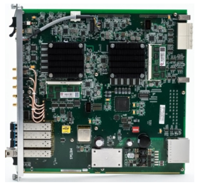 Figure 9 Baseband Card for 4G base station.
There are 10 different supply voltages between 5V and 0.75V, which supply the baseband card. The total current drawn from a 1V supply on one card can reach 40A.
There are various interfaces (CPRI-Common Public Radio Interface, Ethernet, reference clock) up to 4.9 Gbps on the baseband card. There are also various interfaces (hyperlink, serial rapid I/O, SGMII Ethernet) up to 6.25 Gbps among the master and slave processors of the card.
The SoC used in the baseband card has 8 DSP cores (1.2 GHz), 4 ARM cores (1.4 GHz) and 30 application specific coprocessors. Only the hardware documentation required for the hardware design constitutes a 5700 page document set.
There are 1517 pins of the SoC integrated circuit on the baseband card. In order to be able to perform the layout process, advanced production techniques such as blind and buried via, micro via, and bypass via are used.
Layout constraints for fast differential paths such as 10 GHz must be applied very rigidly, taking into consideration both the distances between the differential paths (at most 0.14 mm) and the distances between the source and the target of the signal (at most 0.24 mm). This situation is illustrated in the Figure 10 below.
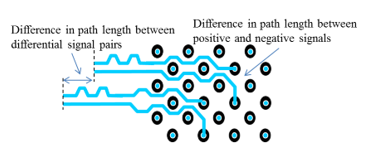 Figure 10 Path length definitions for differential signals.
Layout constraints for fast differential paths of the Baseband Card are illustrated in the Table below. Considering that 1 ps (pico second) is one in a trillionths of a second, and the thickness of the hair is 40 micrometers, it can be seen how difficult the following layout constraints can be achieved.
EMC/EMI precautions for high-speed interfaces must also be held in order for this card to function properly and the relevant processes must be implemented from the beginning of the hardware and mechanical design.
Table Layout constraints for fast differential paths.
| Interface | Difference in path length between positive and negative signals | Difference in path length between differential signal pairs |
| 1 Gbps Ethernet | < 5 ps – 700 mm | < 10 ps – 1.400 mm |
| 4.915 Gbps CPRI | < 5 ps – 700 mm | < 10 ps – 1.400 mm |
| 5 Gbps Serial Data | < 1 ps – 140 mm | < 15 ps – 2.100 mm |
| 50 Gbps Hyperlink | < 1 ps – 140 mm | < 15 ps – 2.100 mm |
4. Design for User Services: Software Design
Today, software has entered into all areas of life without exception. The diversity of emerging technologies and demands makes the software even more complex. The software now communicates more with peripherals and external systems. The development of network structures requires that software be more aware of each other. Manual data transfers over the past years are now done in real time. All of this has increased the compatibility issues of software.
It is said that the progress on hardware follows Moore’s rule. But it is not possible to say that the software fits into this progress. In the early years when the software was growing and becoming more complicated, the designers faced more difficulties than the hardware because the processes were not fully matured [55]. For this reason, most software projects have been delayed for years. As a result, costly and unreliable, hard-to-maintain software is designed for these projects. During this period, software design has entered a crisis period. Hardware costs have fallen while software costs have increased.
Today, new techniques, design methods and tools are developed to control the natural complexity of large software systems. However, software design and test costs still constitute a large part of the design cost of ICT products today.
4.1. Software Development Processes
Companies working in software development are choosing different software development methods ranging from traditional approaches to agile approaches, depending on the needs of the projects they develop. The results of research on methodology selection in software projects show that traditional methods, including the Waterfall model, are still popular, although agile methodologies like Agile Unified Process and Scrum are more common than they were 10 years ago [55]. These surveys have shown that software development organizations also use a hybrid approach based on a large number of methodologies on projects.
Today, widely used software design methods are listed below. One or more of these methods may be preferred depending on the complexity of the software to be developed, the number of software engineers to work with, whether the customer requests are specific, the priority of the documentation, the design time, and whether the system requirements are evident clearly [55].
- Ad hoc
- Waterfall
- Evolutionary Process Models
- Incremental
- Spiral
- Rational Integration Process
- Agile Methods
- Feature-Driven Development
- XP (Extreme Programming)
4.2. Current Trends for Software Development
Today, the complexity of software and the number of developers working on software projects are increasing. In addition, competition in this area is increasing. As the reliability requirements of the software increase, the duration of the project is also shortened. There are various developments in the field of software development, mainly open source code and framework usage, in order to enter the market quickly and cost effectively. This section describes the trends in software development today.
- Open Source Software Development
Open source software is a software model that enables the source code to be reviewed, modified and distributed to third parties for free or for a fee. Today, almost all open source software is available for free. The fee for such codes is usually for additional services such as documentation and guides, technical support, maintenance, etc. provided with the source code of the software [56].
In the 1970s, open source software began to become widespread with the release of an open version of the Unix source code, an operating system with a large user base. This new type of software, which has a license that anyone can edit the source code as they like, has received great interest and has since become widespread.
Open source and traditional software are different in terms of total cost of ownership, flexibility, software quality, security, firm dependency and open standards. In some software products, such as Operating System, Web Browser, Web Server, Web Content Management, Mobile Operating Systems and Applications, the products developed as open source have become bigger market share than their alternatives. Today, the use of open source code has become increasingly widespread due to cost, and faster entry to market advantages.
- Universal & Reusable Software Environments: Frameworks
The Framework contains many software libraries and allows developers to add their own libraries to them. It also guides how the software should be developed. In this way, the designers work with previously tested and reliable software. In addition, the designers can be guided on how to develop the software project to prevent the development mistakes.
Frameworks include libraries as well as design patterns, compilers and test tools. In this way, a development environment is also provided to designers to develop the software project. For example, big chip manufacturers in the embedded design world are no longer just producing chips. These companies also offer software development environments that include customized libraries, compilers suitable for the development environment, and even operating systems for the chips [57].
Chip manufacturers distribute their own product development environments free of charge, in order to promote the use of development environments and to dominate the market. Software project developers choose the framework they need to meet their requirements, leaving the details to the “framework”.
Today, widely used libraries and frameworks are given below.
- a) OpenCV (Open Source Computer Vision Library)
It is a cross-platform library originally developed by Intel for computer vision. Windows and Linux platforms are supported. Since this library includes advanced image processing algorithms, it is possible to develop image processing applications quickly using this library [58].
- b) OpenCL (Open Computing Language)
It is a kind of framework designed to develop programs in heterogeneous systems including CPU, DSP, FPGA, GPU and similar hardware accelerators. OpenCL offers APIs (Application Programming Interfaces) to program and control these processing units. This framework also provides a standard interface for data and task based parallel programming [59].
- c) .NET Framework
It is a software development framework originally developed by Microsoft for Windows installed machines. Using this framework is advantageous for designers who want to develop software on Windows. The use of this framework has now become standard for windows machines. Today, this framework is also attractive to iOS and Linux developers by providing cross-platform support. This platform continues to evolve with the principles: any designer, any application and any platform [60].
- d) Coca Touch
It is a framework, which is developed by Apple to develop applications on iOS (IPhone, IPad), watcOS (AppleWatch) and tvOS (AppleTV) operating systems. Applications developed with this framework can only work on the MAC operating system. These applications are developed with the Objective C ++ language. This “framework” also provides hardware drivers and software support, and applications developed using this framework can be downloaded from the AppStore [61].
- e) ActiveX
This framework is developed by Microsoft and is used to manage downloading of content over the internet. This framework is designed for downloading and updating the software modules over the internet. The first version was released in 1996. Today it is still supported on Windows 10 and by Internet Explorer 11 [62].
- Virtualization
For virtualization, IT (Information Technology) and Telecom sectors have been conducting researches and realizations for many years. Virtualization can be defined as software-based representation of physical resources. The work in this area is focused on servers, data storage devices and communication networks. The goal is to allocate existing physical resources efficiently to services that use these resources, increase service continuity, and reduce installation and operating costs. Because of these advantages, cloud computing applications can be preferred in terms of installation and operating costs, especially with pay-as-you-go model for small and medium-sized businesses. Recently, new concepts such as “fog computing” have emerged in this area [63,64]. In this concept, resources that are used flexibly via the cloud are transported to devices at the edge of the network, for example, to WiFi hot-spot devices, sensors or IoT devices. In this model, approaches such as caching is used to optimize the use of bandwidth, reduce latency and network traffic. In this way, the service quality of the users in the access networks is being improved.
Network function virtualization is a special application of the concept of virtualization to communication networks. In this concept, network functions realized with special hardware are realized with software modules on standard server hardware. This is actually the application of virtualization techniques used in data processing centers to communication networks. Nowadays, this concept can be used in web servers and data processing centers. However, there are some problems to be solved to apply this concept to real-time network devices. The most important of these troubles are high performance requirements and data processing delay variations.
In addition, live migration of network functions between hardware platforms is underway from the point of view of performance of transport time and service interruption time.
The use of this architecture is becoming more widespread as NFV (Network Function Virtualization) technologies reduce investment and operating costs, especially power consumption costs.
- Software Development for IoT (Internet of Things)
Despite the intensive software work for today’s Internet of IoT platforms, a general software engineering approach to systematically developing IoT systems and applications does not exist [65]. So far, researches have been conducted on communication and interoperability issues in this field. Lately, researchers have been working to provide resources and user services with distributed services defined by the software. For example, within the vision of WoT (Web of Things), standard Web technologies are used to provide the development of coordinated IoT services [65]. There are several approaches to interface and programming support for the development of IoT systems and applications. However, work for a common model, methodology and discipline-based approach is still ongoing. There are also work on development environments and development tools in this field.
An article published on this field [66] proposed an IoT middleware that enables IoT systems and the functions of these systems to work together so that the related IoT systems work together. As the technologies used in the IoT become more mature and experience related to the subject grows, it is envisaged that more research on software engineering for IoT systems will be done in the coming years [65].
- Methods for Product Validation & Test
The product validation is performed to verify if the system works correctly, that is if the product meets the specified requirements and standards, and to evaluate differences between the expected and observed results. The testing process begin by determining the requirements in product design and is performed in accordance with the following objectives:
- To ensure product quality
- To reduce re-development costs
- To increase customer satisfaction
The preparations of the test case and the proper setup are vital in order to follow test procedures, appropriately. System analysis and evaluation of the requirements are performed during this preparation step. Cooperation of different teams is vital to evaluate requirements in terms of testability. Any additional activities and required resources to meet the test objectives need to be planned. Possible risks are determined and backup solutions are planned. Test conditions and scenarios, as well as test exit criteria should be defined. A test plan including well-defined steps to follow should be prepared. After the preparation step, the application is taken.
In general, an important class of tests is referred to as box approach [67]. This approach concerns with whether the code or algorithm is tested by taking into account the internal components or only the inputs and outputs. While black-box and white-box approaches have been widely used, gray box approach has received considerable interest in recent years. The black box approach regards the function as a closed structure and is not interested in its design. It is only considered that the right outputs are produced for given inputs. The white box approach checks whether the internal variables and algorithm are appropriate as well as the function works correctly. The gray box approach is related to the design of the test. The gray box tests are applied like the same black box, but the internal data and algorithm structure of the function are considered when the test is designed.
Another point of view, software tests can be classified as follows [68].
- Unit Test
- Integration Test
- Functional Test
- Compliance Test
- Regression Test
- Performance Test
After the errors found in the verification tests are corrected, the test termination criteria are checked. The test is terminated if all criteria are found to be acceptable. After the test is finished, customer acceptance tests are started for the product. The same process is repeated for the faults, additions or changes requested by the customers. After this phase, the customer tests are repeated if necessary, and the test process is terminated.
Competition is increasing due to developments in the ICT sector. On the other hand, the quality of the product is getting more and more important. The importance given to the testing process has also increased for products to be presented to the user with fewer errors. Today, TMMI (Test Maturity Model Integration) model is defined to improve only the test processes, as CMMI (Capability Maturity Model Integration) model that measures software design processes [69].
In the traditional product design process, the first sample production is done at the end of the design and it is tested whether the requirements are met or not. If desired performance cannot be achieved, design change is made by returning to the design process and new sample production is made. The process is completed following this cycle. Constant sample production to test each design leads to both time loss and cost increase. In today’s conditions, the number of initial samples is reduced by computer-aided design. In this way, both the time loss and the cost are reduced. This method is accepted as the modern product design process of today.
- Mechanical Design & Material Engineering
In the mechanical design of the product, various criteria such as material selection, production methods and mold type and its mechanics should be evaluated in computer environment.
In the 1960s, metals were often used as engineering material. In the following years, demand for steel and cast iron was declined, and today generally, two main materials are used in the production of mechanical systems. These are metal and plastic materials. While metal materials are generally used in machining methods, plastic materials are used in injection molding technology [70,71].
Machining is the shaping process by removing material called sawdust from the inside of materials such as metal, plastic and wood. Along with this, unconventional manufacturing methods such as water jet and laser have started to be used.
Plastic molding is a manufacturing method, which involves pouring and shaping a melted plastic raw material into a mold with the help of temperature and cooling and removing it from the mold. Today, plastic materials can be shaped in a very short time.
One of the latest and greatest developments in manufacturing is the three-dimensional printer technology [72]. Although this method is currently used in rapid prototyping, production with this method in the future will not be surprising. Surface roughness cannot be achieved with the existing technology. For this reason, additional processing is required. Moreover, with this technology, very durable products cannot be produced due to the materials they can process.
In recent years, the production of high performance ceramics, polymers and composite industries has developed rapidly. Today, there are more than a hundred kinds of materials, and choosing materials from such a wide spectrum has become a separate engineering subject. Today, in material engineering and researches, various imaging techniques, thermal analysis methods and X-rays are widely used.
7. Manufacturing
Electronic components used in today’s ICT devices are divided into two groups as SMD (Surface Mount Device) and through-hole. The through-hole components frequently used in previous years have been left almost entirely to SMD by the developing technology. The through-hole electronic components must be inserted and soldered in holes in electronic cards. The SMD elements are attached to the card surface and fired.
Surface mounting components can be manufactured much smaller than legged through-hole components [73]. Using small and lightweight components, it is possible to design cards that produce less heat and consume less power. The SMD components can be arranged on both surfaces of the card. Moreover, these components are more resistant to mechanical vibration and shock effects. The weakness of the surface mounting technology compared to the through-hole is the difficulty of manual intervention and repair.
BGA packages offer more pin connections than other SMT (Surface-Mount Technology) package types. For this reason, the BGA package is widely used for components with a high number of pins such as microprocessor and SoC. However, soldering to PCB is much more difficult than other types of packages and requires special stations.
In case of faulty installation, the relevant circuit element is dismounted by local heating method using special devices. At the next stage, the soldering balls are fixed and replaced by local heating under computer control. The BGA rework station is shown below. In this case, a baseband card is reworked for the SoC component.
In BGA packages, the pins are very close to each other and when they are soldered to the PCB, no pins can be seen. A short circuit may occur between nearby pins, resulting in errors during production, or soldering.
BGA surface mount assembly is difficult to test, once it has been assembled. In this case, X-ray devices can be used to control the deformation and fracture of solder balls.
An X-Ray view of the SoC used in a Baseband card is given in Figure 11. In this view, the pins and the connections between them can be clearly seen. At the end of the review, it is confirmed that the pin connections are correct.
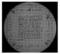 Figure 11 An X-Ray view of the SoC.
7.1. Environment Friendly Approaches for Manufacturing
As the electronic goods sector grows with industrialization and usage habits, the negative effects of electronic waste are increasing rapidly. In order to reduce these effects, environmentally sensitive design has become a mandatory legal requirement. In 2003, the European Union published two important directives for electronic producers. These are Restriction of Hazardous Substances (RoHS) and Waste Electrical and Electronic Equipment (WEEE) directives. These directives are concentrated in two main points. The first is to limit the use of toxic and harmful substances in newly manufactured electronic products and secondly to take into account recycling criteria in product design. In this context, the concept of environmentally friendly design, called eco-design, has emerged. In addition to the traditional design processes, eco-design includes processes from raw material acquisition, product recycling and disposal. For this reason, designers are expected to design by evaluating the recycling and dismount ability criteria of the products [74].
Under the RoHS directive, the use of lead, cadmium, mercury, chromium and brominated components is prohibited. The use of these components in electronic and electrical equipment is causing toxic particles to interfere with the environment. For example, the use of hydrocarbon fluoride to clean the PCB assembly is prohibited because it causes wear on the ozone layer.
8. A Practical Implementation: LTE-Advanced Baseband Unit
In this section, in order to illustrate some of the key features in a cutting edge ICT product design, a LTE-A Baseband Unit (BBU) is considered and the technical competencies, infrastructure and design processes required to develop this product are highlighted.
The first stage for the design of the BBU unit is system-level design, where functional features are derived from the expected characteristics, customer requirements, competitive product analysis and product roadmaps. This step consists of general block design and technical features such as interface characteristics, power supply and cooling. At this stage, it is decided to support some operator specific features in addition to 3GPP Release 10 & Release 11 standards.
The hardware design features of the BBU unit are given in detail in section 3.13. In order to design a high-tech product at this level, advanced technical expertise is required on the high density interconnect PCB production techniques using blind and buried via, micro via, and bypass via. The BBU hardware includes 82 CPU cores and is designed to provide the processing power required by the features specified in the system design phase. This corresponds to a capacity above 1 trillion operations per second. There are 18 CPRI (Common Public Radio Interface) interfaces for radio connections and 2 gigabit Ethernet interfaces for EPC (Evolved Packet Core) connections on this unit. Each radio interface is comply with the CPRI standard.
BBU unit software was developed on a System-on-Chip (SoC) specially developed for Macro Base Station products. Electronics Engineering, Telecommunications Engineering and Mathematical Engineering disciplines have been used together to develop highly optimized and real-time digital signal processing algorithms. BBU software which contains thousands of source files and millions of lines of source code, can be developed with roughly 100 software engineers and many years of design and coding work.
Testing infrastructure which requires tens of millions of dollars in investment cost is required for functional testing of the BBU unit. Using these infrastructures, thousands of functional test scenarios are implemented in the laboratory and in the field. Verification tests of a BBU unit can only be performed using high-tech and complex test equipment, examples of which are given above. For example, in order to use the multi user terminal simulator, it is necessary to examine over 1,000 pages of document and take the training for weeks. Some of the device types included in the test infrastructure required for functional testing of the BBU unit are Multi-user terminal simulators, Channel simulators, EPC (Evolved Packet Core) simulators, Air interface analysers, CPRI (Common Public Radio Interface) test devices, Remote radio units and antennas, Vector signal analyser and generator and Mobile packet analysers.
Finally, ICT products must comply with the relevant hardware, software, product integrity, reliability, environmental and EMC standards. To design LTE-Advanced BBU, tens of thousands of page standard, data sheet and papers have been studied and implemented.
9. Conclusion
Prior to the industrial revolution, goods and equipment to meet daily needs can be produced with simple techniques in small workshops. Later, large factories allowing mass production started to be established and needs for special expertise in various areas of manufacturing techniques have arisen. This trend continued increasingly in mechanical world until 1970s. From the mid-twentieth, first the emergence of transistor and later the invention of the integrated circuit caused a similar development in the electronic world. While in the beginning, mechanical expertise was still predominant in product design, the technical expertise on hardware and software design has become the most crucial parts, in the next two decades.
With the market launch of the first commercial microprocessor, electronic devices started to enter into many areas of our lives. This led to product diversity and consequently to the need for expertise in different areas. Until the 1980s, simple tools for ICT product design and testing were sufficient, but in the next 20 years, more sophisticated design tools and test equipment were required. Nevertheless, the tools and equipment needed to develop an ICT product remained affordable for a start-up company.
After the 1990s, the use of mobile devices in all areas of our lives led to the acceleration of development of technology in the ICT world. Especially, development of display and battery technologies has caused tremendous increase in the use of mobile devices. At the beginning of the new millennium, with the widespread use of internet and video-based services, more bandwidth was needed, which forced new solutions to be developed in cable and wireless communication technologies. However, the emergence of complex modulation techniques to address these demands caused additional hardware requirements, such as faster processors, faster memories, and faster peripheral components.
All of these effects have initiated the key design concepts: smaller, lighter and faster products. Therefore, the dimensions of the components have to be reduced despite the increasing performance and durability requirements. Today lightweight sensors which can be fitted even to swallow birds can be produced, and they can collect and store data for as long as a year. The first commercial microprocessor incorporated 2,300 transistors. Now, new generation processors have around 1.3 billion transistors. Nowadays, the processors produced in the size of one fourth of the 1 cm2 area for wearable devices, deliver 200 times more performance than the processors used in the first PCs. However, with the use of these new technologies in product design, the design process are becoming increasingly complex, engineering skills are becoming increasingly diverse, and the infrastructures needed are becoming increasingly expensive.
In this paper, all the design stages of ICT products are explained. Due to rapid development of hardware technologies, hardware design is getting more and more intriguing. As can be seen in the relevant sections, in order to design an ICT product, very deep technical expertise, expensive development and verification infrastructures are needed in the respective fields.
- C. Hamilton, “A Guide to Printed Circuit Board Design” Butterworth & Co. Ltd, England, 1984.
- E. D. Reilly, “Milestones in Computer Science and Information Technology” Greewood Press, USA, 2003.
- D. Greenstreet, “Enabling multistandard wireless base stations with TI’s KeyStone SoCs” Texas Instruments, Enabling multistandard wireless base stations with TI’s KeyStone SoCs, 2011.
- S. Narnakaje, Z. Lin, “Analysis of LTE Base Station Software Deployment on Multicore SoCs”, Engineers’ Guide to Multicore & Virtualization, s.24, 2012.
- A. P. Sage, Systems Engineering, John Wiley & Sons, Inc., USA, 1992.
- J. Brown, “The History of Printed Circuit Boards – Infographic”, http://www.pcb-solutions.com/pcb-market-monitor/the-history-of-pcb-infographic/
- K. Mitzner, “Complete PCB Design Using OrCad Capture and Layout” Elsevier, UK, 2007.
- H. Johnson, M. Graham, High-speed signal propagation : Advanced Black Magic. Upper Saddle River, New Jersey: Prentice Hall PTR. ISBN 0-13-084408-X, 2002.
- E. Bogatin, Signal and Power Integrity – Simplified, Second Edition. Upper Saddle River, New Jersey: Prentice Hall. ISBN 978-0-13-234979-6, 2009.
- https://en.wikipedia.org/wiki/List_of_device_bit_rates.
- Anritsu, “PAM4 Demands Accurate S-parameters”, 2016.
- H. Huff, Moore’s Law Beyond Planar Silicon CMOS, Springer Series in Materials Science, USA, 2009.
- https://www.extremetech.com/extreme/240901-tsmc-announces-plans-new-16-billion-foundry-push-envelope-5nm-3nm-process-nodes.
- https://www.extremetech.com/computing/221532-tsmc-will-begin-10nm-production-this-year-claims-5nm-by-2020.
- S. Dwivedi, N. R. Prakash, “A Study on Recent Advancements in VLSI Technology using FinFETs” in International Journal of Innovative Research in Science, Engineering and Technology, Vol. 4, Issue 12, 2015.
- S. H. Ok, Y. H. Lee, J. H. Shim, S. K. Lim, B. Moon “The Impact of 3D Stacking and Technology Scaling on the Power and Area of Stereo Matching Processors” in Licensee MDPI, Basel, Switzerland, 2017.
- A Brief History of the x86 Microprocessor, http://www. computerworld.com/article/2535019/computer-hardware/timeline–a-brief-history-of-the-x86-microprocessor.html.
- Graphics Processing Unit, http://www.nvidia.com/object/gpu.html.
- http://www.nvidia.com/object/multi-gpu-technology.html.
- R. Giladi, M. Kaufmann, Network Processors: Architecture, Programming, and Implementation, Elsevier, 2008.
- http://www.nvidia.com/object/tegra-4-processor.html.
- N.Blachford, “Lets Get Physical: Inside The PhysX Physics Processor”, 2006.
- A. Lucian “Google’s Big Chip Unveil For Machine Learning: Tensor Processing Unit With 10x Better Efficiency”, Tom’s Hardware, 2016.
- D. Nenni, P. McLellan, “Fables: The Transformation of the Semiconductor Industry”, 2013.
- http://www.cypress.com/event/psoc-6-purpose-built-iots.
- https://www.xilinx.com/products/silicon-devices/soc/zynq-ultrascale-mpsoc.html#productTable.
- S. Dwivedi, N. R. Prakash, “A Study on Recent Advancements in VLSI Technology using FinFETs” in International Journal of Innovative Research in Science, Engineering and Technology, Vol. 4, Issue 12, 2015.
- http://www.doityourself.com/stry/alkaline-battery-advantages-and-disadvantages.
- J. Bird, Electrical and Electronic Principles and Technology, Sixth Edition, Routledge, 2010.
- J. Lenz, S. Edelstein, “Magnetic Sensors and Their Applications” in IEEE Sensors Journal, vol. 6, no. 3, 10.1109/JSEN.2006.874493, June 2006.
- P. Ripka, M. Janosek, “Advances in Magnetic Field Sensors” in IEEE Sensors Journal, vol. 10, no. 6, June 2010.
- “Modern Magnetic Field Sensors – a Review”, Przeglad Elektrotechniczny, ISSN 0033-2097, 2013.
- M. Andrejasis, “MEMS Accelerometers”, University of Ljubljana Faculty for Mathematics and Physics Department of Physics, March 2008.
- O. J. Woodman, “An Introduction to Inertial Navigation” University of Cambridge Computer Laboratory, United Kingdom, August 2007.
- R. E. Hopkins, F. K. Mueller, W. Haeussermann “The Pendulous Integrating Gyroscope Accelerometer (PIGA) From the V-2 to Trident D5, the Strategic Instrument of choice”in Navigation, and Control Conference and Exhibit Montreal,Canada, 2001.
- R. Mehrotra ,“Thinner, Smaller, Better: Advances in Display Technology” in IEEE MultiMedia,vol. 8, 10.1109/MMUL.2001.939995, 2001.
- J. Gurski, L. M. Quach, “Display Technology Overview”, Lytica White Paper, July 2005.
- F. Okano, M. Kanazawa, K. Hamasaki, M. Sugawara, M. Seino, A. Mochimaru, K. Doi, “Ultrahigh-Definition Television System with 4000 scanning lines “, in NAB BEC proceedings, p.437, 2004.
- K. Aoshima, K. Machida, D. Kato,H. Kinjou, K. Kuga, T. Mishina, “Advanced Display Systems Technologies”,in Industry Applications Society Annual Meeting IEEE , 10.1109/IAS.2013.6682549, 2013.
- S. Methley, W. Webb, S. Walker, et al., 5G Candidate Band Study, Quotient Associates Limited, 2015.
- W. Roh, J. Seol, J. Park, et al., “Millimeter-Wave Beamforming as an Enabling Technology for 5G Cellular Communications: Theoretical Feasibility and Prototype Results” in IEEE Communications Magazine, 52(2),106-113, 2014.
- Z. Liguo, P. Jin, Y. Fang, et al., “A carrier leakage calibration and compensation technique for wideband wireless transceiver” in Journal of Semiconductors, 35(6), 065003, 2014.
- M. Racanelli, P. Kempf, “SiGe BiCMOS Technology for RF Circuit Applications” in IEEE Transactions on Electron Devices, 52(7), 1259-1270, 2005.
- H. Chuang, L. Yeh, P. Kuo, et al., “A 60-GHz Millimeter-Wave CMOS Integrated On-Chip Antenna and Bandpass filter” in IEEE Transactions on Electron Devices, 58(7), 1837-1845, 2011.
- M. Mardiguian, Controlling Radiated Emissions by Design, Springer, Third Edition, USA, 2001.
- X. C. Tong, Advanced Materials and Design for Electromagnetic Interference Shielding, CRC Press, USA, 2009.
- H. Johnson, “Why Johnny Can’t Design a High-Speed Digital System”, University of Oxford.
- https://yearbook.enerdata.net/electricity-domestic-consumption-data-by-region.html#electricity-domestic-consumption-data-by-region.html.
- S. Lambert, M. Pickavet, “Can the Internet Be Greenertor”, in Proceedings of the IEEE, vol. 105, no. 2, pp. 179-182, February 2017.
- Ericsson Mobility Report, https://www.ericsson.com/res/docs/2015/ mobility-report/ericsson-mobility-report-nov-2015.pdf, November 2015.
- http://www.phonearena.com/news/Smartphone-battery-life-over-the-years-A-surprising-study_id82315.
- M.P. Mills, “The Cloud Begins With Coal”, August 2013.
- G. Auer et al., “How Much Energy is Needed to Run a Wireless Network?” in IEEE Wireless Communications, vol. 18, no. 5, pp. 40-49, October 2011.
- J. Wu, Y. Zhang, M. Zukerman, E. K. Yung, “Energy-Efficient Base-Stations Sleep-Mode Techniques in Green Cellular Networks: A Survey”, in IEEE Communications Surveys & Tutorials, vol. 17, no. 2, 2015.
- F.P. Brooks, “No Silver Bullet Essence and Accidents of Software Engineering”, Computer Magazine, vol.20, no. 4, s.10-19, April 1987.
- What is Open Source, https://opensource.com/resources/what-open-source.
- D. Riehle, “Framework Design A Role Modeling Approach” Ph.D Thesis, Swiss Federal Instituteof Technology Zurich, 2000.
- OpenCV, http://opencv.org/.
- The open standard for parallel programming of heterogeneous systems, https://www.khronos.org/opencl/.
- Overview of the .NET Framework, https://msdn.microsoft.com/en-us/library/zw4w595w(v=vs.110).aspx.
- Cocoa Touch, https://developer.apple.com/library/content/documen-tation/General/Conceptual/DevPedia-CocoaCore/Cocoa.html.
- “Introduction to ActiveX Controls”, MSDN, Microsoft. Retrieved June 1, 2016.
- O. Osanaiye, S. Chen, Z. Yan, R. Lu, K. Choo, M. Dlodlo, “From cloud to fog computing: A review and a conceptual live VM migration framework”, in IEEE Access, 10.1109/ACCESS.2017.2692960, 2017.
- N. Iotti, M. Picone, S. Cirani Caligoo, G. Ferrari, “Improving Quality of Experience in Future Wireless Access Networks through Fog Computing” in IEEE Internet Computing, University of Parma, 10.1109/MIC.2017.38,Italy, 2017.
- F. Zambonelli, “Key Abstractions for IoT-Oriented Software Engineering”, in IEEE Software, Volume: 34, Issue: 1, 10.1109/MS.2017.3, 2017.
- M.A. Razzaque et al., “Middleware for Internet of Things: A Survey” in IEEE Internet of Things J., vol. 3, no. 1, 2016.
- N. Li, Z. Li, X. Sun, “Classification of Software Defect Detected by Black-Box Testing: An Empirical Study” in IEEE Second World Congress on Software Engineering, 10.1109/WCSE.2010.28, December 2010.
- E. Suruchi, “Comparative analysis of testing techniques: A Review”, in International Journal of Advanced Science and Research, vol. 1, Issue 5, Page No. 46-50, 2016.
- E. Venendaal, “Test Maturiy Model Integration (TMMi)”, Version 3.1, TMMi Foundation, 2010.
- T. A. Osswald, L.S. Turng, P. Gramann, Injection Molding Handbook, Neuausgabe, 2007.
- M.P. Groover, Theory of Metal Machining: Fundamentals of Modern Manufacturing, John Wiley & Sons, Inc, 2002.
- E. Sachs, M. Cima, J. Cornie, “Three-Dimensional Printing: Rapid Tooling and Prototypes Directly from a CAD Model”, Elsevier, Manufacturing Technology, Volume 39, Issue 1, Pages 201-204, 1990.
- R. Prasad, Surface Mount Technology: Principles and Practice, Springer, USA, 1997.
- P. Knight, O. J. Jenkins, “Adopting and applying eco-design techniques: a practitioners perspective” in Journal of Cleaner Production, s. 549-558, 2008.
No related articles were found.