Design of High Output Impedance, Large Voltage Compliance Output Stage of Implantable Hypoglossal Nerve Stimulator (HGNS) for OSA Treatment

Adv. Sci. Technol. Eng. Syst. J. 5(5), 852–863 (2020);
 DOI: 10.25046/aj0505104
Obstructive Sleep Apnea (OSA) is a potentially common sleep disorder manifested in upper airways’ collapse, either partially or completely. If diagnosed late and untreated, it may result in serious complications. The standard golden method, useful for treating OSA, remains the full night Continuous Positive Airway Pressure (CPAP). Yet, due to the ensuing discomfort it incurs on patients, researchers have been motivated to investigate other efficient alternatives, whereby, OSA can be effectively treated. More recently, an increasingly popular OSA treatment solution has been developed that consists in activating the protrusion muscles of the tongue by stimulating the Hypoglossal Nerve (HGN). After discussing the classification topologies of some neural stimulator output design stages, we consider putting forward the design of output stage of Hypoglossal Nerve Stimulator (HGNS), in compliance with the HGN requirements. The proposed HGNS is simulated in cadence software using the 0.35µm CMOS technology and Matlab software. It proved to enable the delivery of a maximum stimulation current of 1mA through 1kΩ resistive load under 3.3V voltage supply. The output stage managed to achieve large voltage compliance of 94% of the voltage supply and high output impedance of 275MΩ at full scale stimulus current. The total power consumption is about 705.87µW.
1. Introduction
Sleep is a complex neurological state, which has a vital role in maintaining sound health conditions and well-being all along the life. The sleep phenomenon associated significance is clearly manifested in the fact that people usually spend about one-third of their life spans asleep. It is worth noting, in this respect, that according to the third edition of the International Classification of Sleep Disorders (ICSD-3) [1], there exist no less than 83 kinds of sleep disorders. Most common among these disorders is the Sleep Apnea-Hypopnea Syndrome (SAHS).
Indeed, according to the ResMed group [2] report released in May 2018, the SAHS is discovered to affect nearly one billion people worldwide (specifically, 936 million people), ten times greater than the previously released 2007 World Health Organization (WHO) published statics (100 million) [3]. Central Sleep Apnea (CSA) and Obstructive Sleep Apnea (OSA) present the two main kinds of the syndrome. Rated as the rarest kind of SAHS, the CSA is considered by researchers to prevail among fewer than 20% of all subjects affected with this pathology. It usually occurs when the brain fails the transmission of nervous messages to the inspiratory muscles to trigger respiration. As for the OSA, it represents the most widely spread type of SAHS, and is recorded to occur among 84% of syndrome administered analyses [4].
Concerning the present work, we are interested in investigating the OSA type, commonly recognized with recurrent episodes of shrinkage and obstruction of the upper respiratory system during sleep (hypopneas and apneas). As the soft back-throat tissue collapses, the individual struggles harder against the blocked air passage by contracting the tongue and throat muscles allowing oxygen to flow into the lungs. The apnea event lasts for no less than 10 seconds in duration.
Currently, the Continuous Positive Airway Pressure (CPAP) presents the leading OSA therapy mechanism which consists of a mechanical device dubbed that serves to convey a positive flowing of air into the nasal cavities through a facial or nasal mask. The CPAP device has the advantage to maintain, the transmural pressure along the upper airway above Pcrit, thus, preventing apnea episodes from recurring. It is worthing to note that the wear of this mask is not less than 6 hours to achieve the desired purposes. Despite the recognized therapeutic effectiveness of the CPAP [5], patient non-compliance usually stands as an important issue restricting the usage of such a device. Indeed, an elevated flow is needed to get enough positive airway pressure. Such a flow engenders the deterioration of the mucosal functions as it imposes a difficult burden on the nasal mucosa. Subsequently, several complications could befall, e.g., sneezing attacks, allergic rhinitis, and mucosal blockage. In the long-run, the frequent application of the CPAP might well culminate in other negative impacts linked mainly to epidermis issues, such as eye inflammation, the appearance of blemishes on the subject’s face. It is for this reason that 30 to 50% of the CPAP treatment undergoing patients end up with abandoning it throughout the first year of therapy [6,7]. Overall, those with untreated OSA are exposed to significantly severe problems, ranging from hypersomnia to unexpected death [8]. Thus, there is a need for developing a rather effective OSA treatment therapy as an alternative to the CPAP non-compliant patients.
In this respect, pharyngeal dilation via Hypoglossal Nerve (HGN) stimulation has proven to stand as an effective therapeutic approach useful for treating the OSA [9–12]. Accordingly, the motor innervations of the Genioglossus muscle (GG) is the twelfth cranial nerve (XII) which is recognized as the responsible of the tongue protruding and pharynx expansion [13]. The branches associated with the HGN include motor fibers, and an electrical stimulation of those branches helps activate or stir the GG muscle with sensory feedback and then, elevate the tongue to stop the breakdown of the upper airway.
This new therapy is under investigation and in the process of development and completion by multiple groups. In this respect, a comparative study was established among such medical devices as InspireI, InspireII, Apnex, Imthera, and Nyxoah, elaborately treated in [14,15]. The necessity to ensure that the intervention of the HGN stimulator is maintained in such a way as to account exclusively for real apnea events is among the criteria of implant’ reliability. In this regard, it is worthing to highlight that it is required to ensure the detection of real apnea events to avoid damage to the other tongue functions.
In this context, a novel OSA detection method is considered that rests on esophageal Pressure (Pes) signal detection processing [16]. In the relevant literature, this parameter had not been adopted by investigators in OSA monitoring although it is admitted as the gold standard to detect OSA pathology, according to the recent studies [17]. Therefore, the block diagram illustrated in Figure1 is conceived to stand as a promising prospect for future research dealing with the design of medical implants devoted to the treatment of OSA. The architecture involves an internal implantable device coupled with associated external devices. The external devices wirelessly transmit commands and power to the implantable device.
The duty of delivering electrical pulses to the HGN securely and without causing complications of the nerve cells is eventually attributed to the “output stage” or “driving stage”. The HGNS output stage represents a conflict of interest of investigators since it represents functionally the closest part to the biological tissue and any irregularity in HGN stimulation standards may engender tissue damage. The critical aspects, necessary for accomplishing the biomedical and design constraints of the output stage (e.g., large output voltage compliance, high output impedance, low power consumption), usually raise problems as to circuit topology and components. Indeed, Achieving large voltage compliance (ie, very close to the supply voltage), and maintaining high output impedance to keep the desired stimulus current constant disregarding the site and tissue impedances as well as reducing the size and power consumption, have been the major challenges in designing the neural stimulator of output stage circuits to make it more efficient.
In this context, the present work is aimed to put forward a High output impedance, large voltage compliance, and low power consumption output stage for implantable HGNS, specifically conceived to maintain a safe secure treatment of apnea affected subjects and in compliance with the HGN requirements, after discussing the state of the art model topologies relevant to the output stage designs of neural stimulators.
The remainder of this paper is constructed as follows. Section 2 is devoted to depicting the topological classification of neural stimulators, including the related mode, stimulus shape and charge-balanced stimulation techniques. As for Section 3, it involves a thorough description of the proposed HGNS output stage design relevant architecture, with details of the specific blocks they contain. Section 4 is devoted to highlighting the reached simulation results, achieved by means of the cadence virtuoso tool, along with a relevant comparison established with other well recognized output-stage designs. Finally, the major relevant concluding remarks are highlighted in section 5, followed with some propositions for future investigation.
2. Topological classification of neural stimulators
2.1. Stimulus Mode
The output stage of the neural stimulator is responsible for generating electrical stimulation pulses and creating an action potential in the targeted nerve. Generally, the distinct stimulation modes in which the electrical stimulation of nerve cells can be provided are represented in Voltage-Controlled Stimulation (VCS), Charge-Controlled Stimulation (QCS), and Current-Controlled Stimulation (ICS). The entirety of these output stage modes turn out to be bipolar in type so that crosstalk can be reduced, despite the noticeable decrease witnessed in the efficiency parameter. They are usually performed with a Digital-to-Analog Converter (DAC) enclosing binary-weighted transistors or a thermometer code, enabling to control the output signal amplitude and maintain circuit stability.
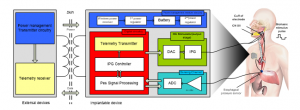
Figure 1: Block diagram of implantable Hypoglossal nerve stimulator.
Concerning the VCS mode, the neural stimulator output is in the form of a voltage, thus, the pulses crossing the tissue demonstrate to depend deeply on the electrode or tissue associated impedance (Ohm’s law). Thereby, the exact charge quantity provided to the electrode and tissue turns out to be ineffectively controlled due to impedance variation. However, this approach has the advantage of maintaining rather high power efficiency [18]. As depicted by Figure 2(a), the DAC current source transistors are implemented under the form of a cascode, so as to raise the output impedance and preserve a constant output current, disregarding the fluctuation of the voltage over the load ZL. Still, the static voltage is beneficial for biasing the cascode transistor, as documented by Sivaprakasam et al. [19] as well as Jones et al. [20]. As for [21], the authors considered that the DAC output impedance can also be boosted by the implementation of an active feedback which biased the cascode transistor.
As regards the QCS mode, the charge, directly delivered to the target tissue, is kept under constant control. The major drawback associated with this method lies in the fact that it occupies a large chip area because of the implementation of numerous switched capacitor networks [22].
With respect to the ICS mode, it is widely applied in implantable neural stimulators, whereby, the stimulated current is not concerned by variations of the tissue load. The model ensures direct control to be kept over the tissue delivered charge by means of linear relationship persistent between charge and current. Accordingly, the mode helps ensure the maintaining of a rather effective control and safer stimulation [23,24].
The current mirror constitutes the most obviously clear mode, whereby, the current-mode DAC output current, IDAC can be duplicated or scaled into output current Iout by means of load. It is worth noting, in this respect, that the Wide-Swing Cascode (WCS) current mirrors are used to help increase the current source output resistance through a gm factor, whereby, gm stands as the trans-conductance of the cascode transistor (M3), as illustrated through Figure 2(b). Noteworthy, also, is the fact that, contrary to the fully cascode current mirror case, the external voltage Vbias is used for biasing the WSC circuit stacking transistors. Accordingly, regulating the biasing voltage Vbias contributes to the reduction of the headroom voltage to 2VDsat. As regards voltage compliance, it is reduced to VDD-2VDsat .

Figure 2: (a) “Folded cascode” FC current mirror with output impedance boosted via active feedback; (b) “Wide-Swing” WS Cascode current mirror, entirely controlled via DAC current mode.
2.2. Stimulus Shape
It is worth highlighting that there exist two commonly recognized stimulus waveforms, widely applied in the field of neural stimulation, namely, the monophasic stimulus form and the biphasic stimulus one.
Regarding the monophasic waveform, it is characterized with a unidirectional pulse, more frequently applied in surface electrode stimulation process, as depicted through Figure 3(a). Noteworthy, however, is that monophasic stimulation culminates in irreversible damage to the biological tissue, because of the charge accumulation on the electrode-tissue interface.
This problem may be prevented by implementation of biphasic stimulation. Indeed, each pulse in the charge-balanced biphasic stimulation process is followed with an inverse polarity pulse, culminating eventually in a succession of a cathodic (negative) phase, succeeded by an anodic (positive) phase, as demonstrated by Figure 3(b). The cathodic phase serves to depolarize nearby axons and triggers the potential action permitting to excite the muscle response. The succeeding anodic phase undertakes to neutralize the primary phase accumulated charge by reversing the damaging electrochemical process, likely to occur at the level of electrode-tissue interface throughout the cathodic phase. The time delay, slightly separating the two stimulation phases, is dubbed interphase gap. Hence, the anodic phase does not impede the action’s potential propagation triggered by the cathodic phase. It is for this reason that the biphasic stimulation procedure is considered safer than the monophasic stimulation procedure, which makes it widely applied and fit for application in neural stimulators to prevent tissue damage [23–25].
Generally, the square pulse (active), supplied by active circuits, turns out to be the stimulus more suitably fit for application in the cathodic phase, while the ensuing anodic phase can be either square or exponentially decaying (active or passive discharging), as illustrated through Figure 3(c), below.
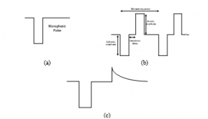
Figure 3: (a) A typical monophasic-stimulus pulses; (b) A symmetric biphasic-stimulus pulse with active-cathodic and passive-anodic phases; (c) A Biphasic stimlus pulse with active-cathodic phase and passive-anodic phases (exponential decay).
2.3. Charge-balanced stimulation
One of the well-established principles of neural stimulation is the achievement of charge balancing among the different stimulus pulses related phases throughout the execution of stimulation process. It is a protecting measure that helps avoid the accumulation of the charge in the biological tissue, likely to result in the rise of electrode potentials to levels inducing water hydrolysis to start. Actually, there exist several reasons for a charge imbalance to take place, mainly, a semiconductor breakdown, current leakages due to cross-talks among neighboring stimulating positions, and wire breakdown. The correction and the generation of the charge imbalance are ensured noticeably by connecting in series the blocking capacitor with each stimulating electrode. Figure 4, below, illustrates three current-mode stimulator configurations deploying a blocking capacitor [26]. The nerve tissue is sited between both of the anodic (A) and the cathodic (C) electrodes, denoting a polarity that indicates the stimulus pulse.
As for the Figure 4(a) depicted circuit [21], the cathodic electrode remains perpetually associated with a reference voltage, usually both of the supply voltages associated midpoint. The cathodic and anodic relevant current supplies are respectively generated by the programmable current sink IstimC and current source IstimA. These current supplies are driven through the load, representing the nerve-electrode impedance, by the control of switches S1 and S2.
Regarding the case in which only a single supply is available, as illustrated through Figure 4(b), both of the anodic and cathodic current supplies turn out to be generated from a single current sink Istim, by inverting the current paths through the S2 switch. Both of the Figure 4(a) and 4(b) displayed configurations indicate charge-imbalance provided solutions. Yet, reaching accurately zero net charges following each stimulation period is not practically feasible owing to the mismatch of timing errors and leakage emanating from nearby stimulating sites. Hence, incorporating the switch S3 seems imposed to help in periodically removing the residual charge by generating an extra passive discharge phase.
As the circuit configurations appearing in Figure 4(a) and 4(b) necessitate the incorporation of the third phase, some investigators consider deploying the passive discharge phase as the principal anodic phase, as clearly described through the Figure 4(c) depicted circuit illustration [27].
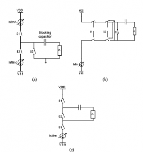
Figure 4: Current-mode stimulator configurations deploying blocking capacitor: (a) dual supplies with active cathodic and active anodic phases; (b) Single supply with active cathodic and active anodic phases; (c) single supplywith active cathodic phase and passive anodic phase.
In general, blocking capacitors stand as critical tools significantly useful for ensuring that DC current cannot, by any means, pass into the electrodes in the event of semiconductor failure resulting from voltage failure or current leakage. More specifically, they are typically considered as off-chip surface-mount components given their highly required value (of a few microfarads in the case of lower-body application stimulators). As for applications in which blocking capacitors are not applicable, due mainly to physical size constraints, other active charge-balancing alternatives turn out to be imposed. In this respect, Sit et al. [28] considered investigating the “Dynamic current balancing” method.
As Figure 5 (a) depicted circuit indicates, the current sink and the PMOS transistor (M1) are respectively responsible for generating both of the cathodic and the anodic phases. Firstly, both of the Scathodic and Sanodic switches are on, while the two sampling switches, Ssamp, are off. When the circuit sets the drain current amplitude of M1 to equate the current sink (as a feedback effect), the resultant bias voltage Vbias affect on the M1 gate turns out to be sampled and held. After that, the two Ssamp switches are on and Scathodic switches off to generate cathodic current. Then, Scathodic switches on and Sanodic switches off. As the gate voltage of M1 is held at Vbias, an anodic current, of an amplitude equal to that of the (cathodic) sink, goes through Sanodic to the load. According to Ortmanns et al. [29], the “Active charge balancer” method offers the advantadge of providing feedback information about the electrode condition after stimulation.
In the Figure 5 (b) figuring circuit, the extra voltage acquired following a biphasic pulse, is measured and compared to a safe referential benchmark voltage. Should the electrode voltage prove to surpass the safe window, supplementary short stimulation current pulses need be applied to drive the electrode voltage towards a balanced condition. In an attempt to experiment with a rather effective charge-balancing method, Williams et al. conducted a special study [30] relying on the implementation of an “H-Bridge” circuit.
Accordingly, the same current source could be applied to both phases (thus, doing away with the mismatch factor). The current path, as flowing through the electrode, is merely switched/driven, as illustrated through Figure 6. Throughout the cathodic phase, φ2 is high with current flowing from electrode B to electrode A. As regards the anodic phase, φ1 is high and the current is flowing from electrode A to electrode B. This technique assumes the persistence of an asymmetrical biphasic waveform maintaining a delay between the cathodic and anodic phases.
The architecture has been demonstrated to offer a number of valuable benefits, particularly, decreasing the power consumption range, while initiating action potentials at significantly lower charge thresholds [31], thus, enhancing safety stimulus.
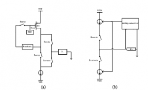
Figure 5: Charge balancing relevant methods: (a) Dynamic current balancing; (b) active charge balancer.
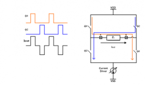
Figure 6: H-bridge architecture highlighting the control of bi-directional current flow insured by Switches, passing through the load ZL.
3. Design of HGNS Output Stage
In this work, the ICS stimulus architecture was opted for as the most optimally fit stimulation pulse generating framework on which the present work is based, rather than the other stimulation modes detailed in the preceding section (i.e., the VCS and QCS).
The conceptual block diagram of the proposed HGNS output stage is described on Figure 7, below. The output stage englobes two main parts. The first current driver part encloses the DAC of type low-voltage, binary-weighted 6-bit current mode and a performing current mirror, while the second part consists in the switch network configuration which provides the generation of biphasic current pulsations by alternating the flow path of the stimulated current, passing within the targeted tissue, as already stated.
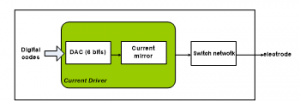
Figure. 7: Conceptual block diagram of the proposed implantable HGNS output stage.
3.1. Current pulse generator design
- Current Steering Digital-to-Analog Converter CS-DAC
A specific binary-weighted 6-bit Current-Steering Digital to Analog Converter (CS-DAC) is employed in the proposed neural stimulator output stage. Actually, this topology has proved an important capacity to direct conversion without the necessity for a voltage stage. Besides, it guarantees high speed, a small chip-area, and maintains a minimally low power dissipation [32,33].
Figure 8 highlights the advanced CS-DAC circuit, whereby, all the transistors are performing in the saturation region. The circuit of reference current, illustrated on Figure 8(b), provides the reference current types Iref1 and Iref2 (8 Iref1), drawn from a reference current Iref of 2.54µA, that are mirrored into transistors M2 and M3. Given the respective sizes of M3 (m=8, W=11,52µm, L=0.35µm) and M2 (m=1, W=1.44µm, L=0.35µm), as figured in the circuit, the drain current of M3 turns out to be 8 times greater than that of M2. In effect, maintaining the same dimensions for M4 and M5 as the transistors M2 and M3, respectively, culminates in having the same drain-source voltages of both transistors M2 and M3. The accuracy of the current copier circuit is proved to be improved by applying this strategy. Figure 8 (a) showed that the currents passing through the drains of the transistors M4 and M5 are mirrored by the transistors M6 and M10 on the left and right sides of the CS-DAC, respectively. The gates of the transistors (M6-M9) and the transistors (M14-M17) are inter-connected to ensure saturation and controlled polarity voltage. This measure is aimed to help in saving and conserving power to the maximum. The PMOS transistors’ width range adapts to the copied current in conformity with the size of the reference branch transistors.
It is also worth mentioning, in this respect, that employing a 6-bit binary-weighted CS-DAC composed of transistors that have the same dimensions in both sides helps remarkably in saving the area of the integrated circuit. Once there is no stimulation current is produced, the transistor Mstim1 is implemented to serve in switching off the proposed CS-DAC. Therefore, it plays the role of power conserver when the design is in the mode “stand by”. By switching on Mstim1, the input digital codes (D0-D5), which represent the addition to the 6 branches through applying the law of knots, undertake to control CS-DAC total output current. Accordingly, the bits D0 and D5 designate to the Least Significant Bit (LSB) and the Most Significant Bit (MSB), respectively. In the CS type of DAC, PMOS transistors are responsible for monitoring each current source indexed by ‘i’. The current related to this source is Ii = 2i.Iref, where, Iref signifies the current reference by a reference current generator. It also stands for the LSB current Iref = ILSB. At a given moment ‘t0’, if the digital input , is recognized, the total output current of the CS-DAC Iout provided to the following module (current mirror) is expressed as follows:
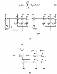
Figure 8: The proposed DAC associated (a) schematic circuit; (b) reference current generator.
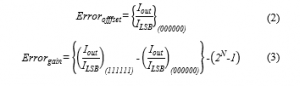
The static absolute accuracy of the proposed CS-DAC can be described in relation to three fundamental error types, i.e., offset errors, gain errors, and linearity errors. The offset error is defined by a persistent shift in the transmission characteristic of the DAC. Indeed, when the digital input D equal to “000000”, the ideal output current must be equal to 0A. If the analog output is unequal to zero, an offset error will be observed. Concerning the gain error, it stands for the difference of the real slope and the perfect slope of the CS-DAC transfer feature. It appears to continue when the slope of the best-fit line by the real transfer characteristic of the DAC is different from the slope of the best-fit line by the ideal one. With respect to the current study case, both of the offset and gain errors are determined by means of the two equations below:
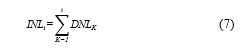
Still, we are mainly interested in these two static specifications: Integral Non-Linearity (INL), or relative accuracy as well as Differential Non-Linearity (DNL), which are most highly recognized in the ac performance. The difference calculation of each level from the real and ideal widths presents the Differential nonlinearity. Considering the ideal output value of a certain code is expressed by: = , the real value generated by the CS-DAC to the same code is: = . Thus, deviation is directly provided by:

In this context, DNLi is attributed to the noticeable difference that exists between two variations in a given transitional code, such as:
![]()
The positions of the ideal output current are distinct from the positions of the real output current. This difference appearing between both of them defines the INL. It is also characterized with the accumulation of previous DNL errors, as highlighted through the expression below:
The main drawback of the weighted binary CS-DAC design lies in the persistence of glitches due to the delays caused by the switch of varying currents. These glitches can well engender a reduction in the system’s respective dynamic performance [34].
- Regulated cascode current mirror
The regulated cascode current mirror is responsible for performing an accurate conveyance of stimulus current to the switch network. It is designed for the purpose of effectively satisfying the biomedical micro-stimulations associated key requirements, such as low voltage operation, high output impedance, and large voltage compliance. Long-channel transistors were applied in the cascode topology for increasing the output impedance value. Furthermore, to ensure large voltage compliance, the implemented output transistors should be characterized by high channel widths for limited overdrive voltage. For a voltage compliance benefiting from the maximum amount of voltage supply to take place, a compromise has been introduced in the design of the current mirror. The schematic diagram of the cascode current mirror, figuring in Figure 9 (a), appears to involve a low voltage (Vb = 0.25V), which ensures the voltage to drop conveniently to fit for the circuit operation (voltage headroom) and regulate the power consumption. The bias voltage Vb is determined by the saturation voltage condition (Vgs – Vth ≤ Vds), once M22 and M23 are discovered to operate in a saturation region. The four (M22 to M25) transistors bear the same dimensions for a unit gain (25u/1.1u). The concept of this regulated cascade current mirror consists in increasing output impedance of the proposed CS-DAC through assuring the bias of the cascade transistor M24 by active feedback using an Operational Transconductance Amplifier (OTA), as schematically depicted through Figure 9 (b). Applying active feedback serves to ensure that the drain associated with the mirror transistor M25 is held at some constant voltage in a feedback loop to equate the drain voltage associated with M23 (i.e., the OTA should be in the role of voltage follower). The output resistance associated with the regulated cascode current mirror circuit is provided by:
![]()
Where: A denotes the OTA gain; r025 designates the output resistance associated with M25 and gm24, and r024 stands for the transconductance and output resistance of M24, respectively. The voltage compliance is expressed by:
![]()
Where: Vgs22 stands for the gate source voltage of M22 and VoD24 represents the overdrive voltage of M24. VoD has been defined as the voltage persistent between the transistor gate and source (Vgs) in excess of the threshold voltage (Vth). It can be determined by the difference outcome perceived between both parameters (VoD = Vgs – Vth). As highlighted by (9), Vb is expected to be elevated to provide large voltage compliance. The transistor M25 may be driven summarily into the triode region due to the boost of Vb, thus, automatically reducing the output impedance. The maximum value for Vb is equal to VDD-Vgs22-VoD25, which brings about a voltage compliance of VDD-VoD24 -VoD25.
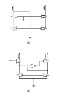
Figure 9: (a) Schematic diagram highlighting the cascode current mirror circuit. (b) The cascode current mirror with active feedback to boost output impedance.
The active feedback insured by the amplifier should allow high input common-mode voltages, and provide sufficient gain useful for reaching a high-level of output impedance. The topology of a single-stage folded-cascode OTA with NMOS input transistors has been designed to fulfill these requirements, as shown through Figure 10. Accordingly, the output impedance is equal to:
![]()
Where: A denotes the OTA provided gain; gm27 represents the transconductance of transistor M27; r27 designates the output impedance of M27 transistor, and r26 refers to the output resistance of M26 transistor.
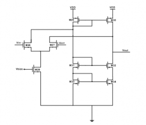
Figure 10: Folded cascode OTA.
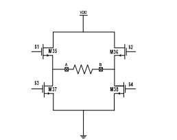
Figure 11: Block diagram of the bi-directional current generation as based on ‘H bridge’ architecture.
3.2. Switch network configuration
Delivering a bi-directional stimulated current by the output stage of HGNS is preferred than the mono-directional current to the cuff of electrode since it prevents any charge cumul in the biologic tissue. Figure 11 displays the switch network configuration, based on ‘H bridge’ architecture. This architecture is applied in power-efficient shapes, where a single the full stimulation back-end is functioning under a single-rail supply voltage and only one a current source is disposed. The switches (S1-S4) serve to guide current within the biological tissue in the requested direction. Activating these switches makes the current circulate in a certain sense whereas turning on the other pair of switchers (S2-S3) orientates the current towards the opposite sense. It follows, therefore, that only a single current source turns out to be needed to make the stimulation current bi-directional. As to the resistance (R) figuring on the schematic diagram, it reflects the similar impedance of the recognized biological tissue between the cuff of electrode. Concerning the switches S5 and S6, they are in charge of grounding the stimulation sites. This mission consists in supplying a special pathway in order to discharge the extra charge caused by the imbalance between the anodic and cathodic periods to prevent any possible tissue damage.
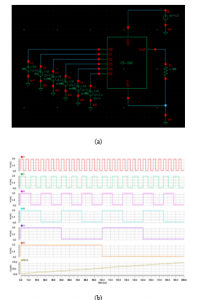
Figure 12: (a) Test bench of 6 bits CS-DAC. (b) The CS-DAC related binary input.
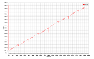
Figure 13: Output Current of the proposed binary weighted CS-DAC.
4. Results and Discussion
4.1. Stimulation results
The performed simulation stage and the relating reached results are achieved by means of Cadence Virtuoso tool for CMOS 0.35μm process technology, under 3.3V supply voltage. Figure 12, below, displays the Test Bench of 6bit CS-DAC along with its input digital codes (D0, D1, D2, D3, D4, D5) ranging from ‘000000’ to ‘111111’. The resolution of a CS-DAC refers to the number of unique output current levels the converter is able to produce.
In the case of HGNS, a CS-DAC with a resolution of 6 bits is needed, since it enables to produce a range of 64 different current levels at its output. Therefore, operating on a 6-element binary code is sufficient for providing a flexible generation of electrical pulses and helping to save significant chip-area. Indeed, the transient response of simulated output current, associated with the proposed CS-DAC, is discovered to be relatively monotonic, as illustrated through Figure 13, below.
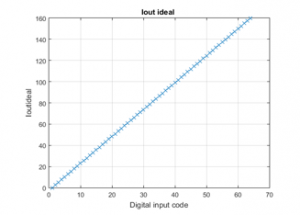
Figure 14: Ideal output current versus DAC input codes.
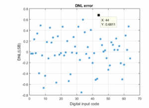
Figure 15: DNL error.
At this level, Matlab software is used for the purpose of determining the proposed CS-DAC associated static performance. The ideal conversion of the digital codes to the current output is depicted on Figure 14. As for the Figure 15 and 16, they respectively indicate the relating DNL and INL performance. The attained results prove to reveal well that the DNL is comprised between -0.669 and +0.681LSB, and that the INL is within -0.563 to +0.815LSB. The proposed DAC associated specifications are depicted on the Table 1, below:
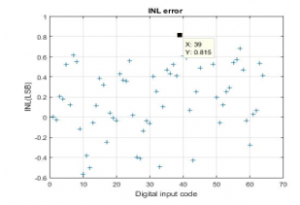
Figure 16: INL error.
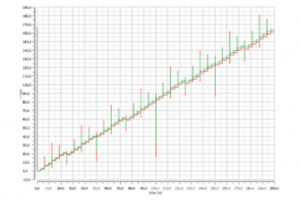
Figure 17: Input and output current concerning the regulated cascode mirror.
Table 1: Performance of the proposed DAC
| Parameters | DAC obtained |
| Supply Voltage (V) | 3.3 |
| Approach | Current steering |
| Resolution (bits) | 6 |
| Temperature (°C) | 27 |
| Conversion Rate | 50 |
| Full Scale Current (µA) | 161.05 |
| LSB Size (µA) | 2.54 |
| DNL (LSB) | -0.669≤INL≤+0.681 |
| INL (LSB) | -0.563≤INL≤+0.815 |
| Gain error (LSB) | +0.37 LSB |
| Offset error (LSB) | 3.9 10-4 LSB |
| Power dissipation (µW) | 89.529 |
As mentioned in the previous section, the current generator requires a minimum of two steps to convert the input digital bits into the output stimulus current. The digital bits are first converted into an analog current which is applied later to a cascade current mirror. The transient response of the input and output current of the regulated cascode mirror is displayed on Figure 17. Given the imposition of sufficient linearity and adequate transition time of the stimulation current, it is legitimate to ascertain the circuit flexibility. The role allocated to this current mirror lies in raising the DAC output impedance through employing active feedback using an operational trans-conductance amplifier (OTA). As already stated, this OTA bears an NMOS input folded cascode configuration, and helps consume a bias current of 0.88μA. Figure 18 reveals the frequency response relevant to the proposed folded cascade OTA. Based on this figure, the circuit proves to be able to obtain 74dB with a frequency bandwidth of 69 MHz at an input common-mode voltage range of Vin = 250mV. The performance of the folded cascode OTA is depicted on Table 2, figuring below.
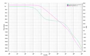
Figure 18: Gain and phase response of AC analysis for the OTA folded cascode.
Table 2: Custom design performance of the proposed OTA
| Specifications | Values |
| Supply Voltage (V) | 3.3 |
| DC gain (dB) | >70 |
| GBW(MHz) | 69 |
| Phase Margin(degree) | 30 |
| Settling Time (µs) | 1 |
| Slew Rate (V/µs) | 4 |
| ICMR (V) | 1.5-2.5 |
| CMRR (dB) | ≥60 |
| Output Swing (V) | 1-2.8 |
| PSRR (dB) | ≥60 |
| Power consumption (µW) | 213.9 |
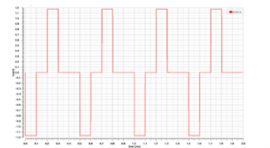
Figure 19: A train of biphasic current pulses.
The operation of generating rectangular biphasic pulses to the load rests heavily on the H-bridge switch network configuration. With respect to the HGNS case, the stimulation charge to the neural tissue of the twelfth cranial nerve needs to be within the range of 0.5mA to 2.5mA, so as not to damage the other tongue-associated functions. The output stage should be implemented in compliance with a resistive load model, with an impedance rate ranging between 200 and 3KΩ [35]. Figure 19 illustrates the stimulus current pulses under 1k resistive load relevant to four complete stimulation cycles. The stimulation period is set to 500μs with 100μs interphase delay which presents a pause between the cathodic and the anodic phase. The HGNS proves to be capable of providing 1.17ms deliverable stimulus current under 3.3V voltage supply. It exhibits a voltage compliance of 3.1V along with an output resistance of 275 MΩ at full scale stimulus current.
4.2. Comparison with relevant output stage stimulators designs
At this level, a comparison is established with other output stage circuits used in Functional Electrical Stimulation (FES) applications, as figuring on Table 3. Accordingly, a respective summary of the entirety of the relevant aspects is depicted, including the related mode, topology and stimulation parameters. Initially, the aim was to establish a comparison with a number of already advanced OSA disease treating neural-stimulator designs. Nonetheless, neither the related specifications, nor the associated performance of the proposed schemes have been available in the relevant literature. In this respect, Velloso and Souza [36], Chen et al. [37] as well as Cheng et al. [38] designed circuits based on the implementation of a transistor that serves to create a High voltage output in the secondary side of the step-up transformer by switching its primary winding. In turn, the design of the output stage, advanced by Lima and Cordeiro [39], Yochum et al. [40], and Khosravani et al. [41], put forward a common specification, namely, the implementation of a current mirror, whereby, the output current can be regulated. As for Masdar et al. [42], they envisaged the use of LM675 power operational amplifier, operated by a DAC and microcontroller, to produce biphasic impulses with a changeable extent. As for Willand and De Bruin [43], they inserted TIP 50 a high voltage bipolar transistor, activated by means of an operational amplifier, as part of their envisioned output-stage design. With respect to Qu et al. [44], they constructed their proper stimulator output-stage architecture on the basis of an H-bridge switch network, which turns out to involve four controlled switches. Concerning Brunetti et al. [45] elaborated study, a high voltage op-amp (PA78) was adopted, which is considered as a voltage-to-current amplifier, able to generate biphasic current pulses. Regarding Huerta et al. conducted study [46], it rests on the idea of reducing charge accumulation in the biological tissue. To this end, they considered applying special switch-capacitor (SC) converters that produce zero net charge elevated slew-rate impulses, thus, decreasing the feeling of pain. This concise literature review reveals well that, in their greatest parts, the advanced transformers, designed for implementation in voltage-controlled output stages, appear to rest predominantly on the idea of easily increasing voltage levels. They were also liable to provide biphasic stimulus whenever the output stage proves to involve a center tap. Hence, based on this abrupt summary, one could well note that most of the investigators seemed to adopt biphasic current pulses as an effective stimulation topology useful for reducing the undesirable effects of charge accumulation on the biological tissue. In addition, symmetric circuits enclosing an H-bridge configuration proved to exhibit an important safety characteristic, as scientifically demonstrated by relevant research studies. It is in this context that the present research can be set, motivated mainly by the interest to investigate a special design of the output stage construct that rests on a biphasic current stimulation architecture equipped with an H-bridge switch network, relevant to the treatment of OSA disease.
Table 3: Review of the output stage related circuit specifications as figuring in the relevant literature
| Research
Work |
Stimulation
Mode |
Output
Topology |
Stimulation
Parameters |
| Velloso and Souza
[36] |
I |
Biphasic |
PW: 50 – 500 μs |
| f: 20 – 200 Hz | |||
| I: 0 – 100 mA | |||
| Chen et al.
[37] |
V |
Monophasic |
PW: 20 – 400 μs |
| f: 40 Hz | |||
| V: up to 150 V | |||
| Cheng et al.[38]
|
I |
Biphasic |
f: 200 Hz |
| I: 100 mA | |||
| Lima and Cordeiro
[39] |
I |
Monophasic |
PW: 50 μs – 1ms |
| f: 1 – 10 Hz | |||
| I: 0 – 100 mA | |||
| Yochum et al.[40] |
I |
Monophasic/Biphasic |
PW:100 – 600 μs |
| I: 100mA | |||
| Khosravani et al.[41] |
I |
Monophasic/Biphasic |
f: 50 Hz |
| I: 0 – 150 mA | |||
| Masdar et al.[42] | I |
Monophasic/Biphasic |
PW: 10 – 500 μs |
| I: 10 – 120 mA | |||
| Willand and De Bruin[43] | I |
Monophasic |
PW: 5 ms |
| f: 20 Hz | |||
| I: up to 22mA | |||
| Qu et al.[44] | I | Monophasic/Biphasic | I: 150 mA |
| Brunetti et al.[45]
|
I |
Biphasic |
PW:10 μs – 5 ms |
| f: 0 – 100 Hz | |||
| I: 0 – 120 mA | |||
| Huerta et al. [46] |
V |
Biphasic |
PW:10μs –10ms |
| f :1 Hz – 15KHz | |||
| V: up to 300 V | |||
| The present design |
I
|
Biphasic |
PW: 100 μs |
| f: 2 KHz | |||
| I: 0 – 1.17 mA |
*N.B: the relevant denotations are: f: frequency; I: current; V: voltage; PW: Pulse Width.
Table 4 reports the comparison of Performance summary between the proposed HGNS output stage and other works published in the literature.
Table 4: Performance comparison with previous works
| Properties | [24]
M.Azin |
[47]
R.Shulyzki |
[48]
S.Farahmand |
This Work |
| Technology (µm) | 0.35 | 0.35 | 0.18 | 0.35 |
| Output impedance (MΩ) | >45 | NA | 160 | 275 |
| Compliance voltage (%) | 94 | 87 | 94 | 94 |
| Power consumption (µw) | N/A | 750 | 816 | 705.87 |
| Stimulation Mode | Current | Current | current | current |
| Supply voltage (V) | 5 | 3 | 1.8 | 3.3 |
| Resolution (bits) | 6 | N/A | 6 | 6 |
5. Conclusion
More recently, current OSA pathology treatment concepts turn out to rest on the idea of therapeutic electrical stimulation of the HGN. For this reason, a special architecture of the implantable HGNS was investigated. The stimulator output stage constitutes the most significant part of the implantable stimulator system, given the fact that it is connected directly with the biological tissue, in addition to its responsibility for triggering the stimulated nerve’ potential action. In this regard, an overview of existing topologies relevant to the architecture of neural stimulator output stages was provided, considering the stimulation mode, shape and safety measure characteristics. To this end, an output stage of implantable HGNS has been designed using standard 0.35µm CMOS technology. The goals of such architecture were focused on satisfying low voltage biomedical stimulators constraints fit for HGN stimulation. It proved to achieve an efficient performance comparing to the other output stages of stimulator design. Indeed, the proposed output stage design was able to show large voltage compliance of 3.1V under 3.3V power supply, high output impedance of 275MHz, and consuming an amount of low power consumption of the rate of 705.87µw. It permits the delivery of a maximal stimulation current of 1.17mA to the targeted tissue across a 1KΩ resistive load. As future work, the issue of communication between the pacing module (as a proposed design of output stage HGNS) and sensing module (Pes signal processing ), which is already treated as part of a previously conducted work is envisaged to investigate. Hence, as the stimulated current pulses’ intensity proves to depend highly on the severity of esophageal pressure amplitude decreases, the proposed HGNS architecture, depicted on Figure 1, could well stand as a key design that paves the way for the creation of new generations of HGNS.
Conflict of Interest
The authors declare no conflict of interest.
Acknowledgment
The authors are deeply grateful to Professor: ABDELMOULA Mohamed, Chief of the Maxillo-Facial Surgery Department of the CHU Habib BOURGUIBA University Hospital, Sfax, as well as to Dr. TURKI Mohamed pulmonologist, President of the Tunisian Society of Sleep Medicine (STMS) organization, for their direction, fruitful recommendations, and valuable aid in matters of relating issues.
- M. J Sateia, “International classification of sleep disorders-third edition highlights and modifications,” Chest, 146(5), 1387–1394, 2014, doi:10.1378/chest.14-0970.
- ResMed – Newsroom, The Lancet Publishes: More Than 936 Million Have Obstructive Sleep Apnea Worldwide | Resmed Inc, 2019.
- J. Bousquet, N. Khaltaev, eds., Global surveillance, prevention and control of chronic respiratory diseases: a comprehensive approach, WHO Organisation, 2007.
- I.T. Morgenthaler, V. Kagramanov, V. Hanak, P. A Decker, “Complex Sleep Apnea Syndrome: Is It a Unique Clinical Syndrome?,” Sleep, 29(9), 1109–110, 2006, doi:https://doi.org/10.1093/sleep/29.9.1109.
- J. Guo, Y. Sun, L.-J. Xue, Z.-Y. Huang, Y.-S. Wang, L. Zhang, G.-H. Zhou, L.-X. Yuan, “Effect of CPAP therapy on cardiovascular events and mortality in patients with obstructive sleep apnea: a meta-analysis,” Sleep and Breathing, 20(3), 965–974, 2016.
- T. E. Weaver, A. M.Sawyer, “Adherence to Continuous Positive Airway Pressure Treatment for Obstructive Sleep Apnea: Implications for Future Interventions,” The Indian Journal of Medical Research, 131, 245–258, 2010.
- I. Smith, V. Nadig, T. J.Lasserson, “Educational, supportive and behavioural interventions to improve usage of continuous positive airway pressure machines in adults with obstructive sleep apnoea,” Cochrane Database of Systematic Reviews, 2, 2009, doi:10.1002/14651858.CD007736.
- T. Young, L. Finn, P. E. Peppard, M. Szklo-Coxe, D. Austin, F.J. Nieto, R. Stubbs, K.M. Hla, “Sleep Disordered Breathing and Mortality: Eighteen-Year Follow-up of the Wisconsin Sleep Cohort,” Sleep, 31(8), 1071–1078, 2008, doi:https://doi.org/10.5665/sleep/31.8.1071.
- A.R. Schwartz, D.C. Thut, B. Russ, M. Seellagy, X. Yuan, R.G. Brower, S. Permutt, R. A. WISE, P. L.SMITH, “Effect of electrical stimulation of the hypoglossal nerve on airflow mechanics in the isolated upper airway,” American Review of Respiratory Disease, 147(5), 1144–1150, 1993, doi:10.1164/ajrccm/147.5.1144.
- D.W. Eisele, A.R. Schwartz, A. Hari, D.C. Thut, P.L. Smith, “The Effects of Selective Nerve Stimulation on Upper Airway Airflow Mechanics,” Archives of Otolaryngol Ogy-Head & Neck Surgery, 121(12), 1361–1364, 1995, doi:10.1001/archotol.1995.01890120021004.
- W. Hida, H. Kurosawa, S. Okabe, Y. Kikuchi, J. Midorikawa, Y. Chung, T. Takishima, K. Shirato, “Hypoglossal nerve stimulation affects the pressure-volume behavior of the upper airway.,” American Journal of Respiratory and Critical Care Medicine, 151(2), 455–460, 1995, doi:https://doi.org/10.1164/ajrccm.151.2.7842206.
- A. Oliven, R.P. Schnall, G. Pillar, N. Gavriely, N. Odeh, “Sublingual electrical stimulation of the tongue during wakefulness and sleep,” Respiration Physiology, 127(2–3), 217–226, 2001, doi:https://doi.org/10.1016/S0034-5687(01)00254-7.
- H. Zhang, J.-Y. Ye, L. Hua, Z.-H. Chen, L. Ling, Q. Zhu, L.-M. Wang, L. Zheng, Y.-H. Zhang, “Inhomogeneous neuromuscular injury of the genioglossus muscle in subjects with obstructive sleep apnea,” Sleep and Breathing, 19(2), 539–545, 2015, doi:https://doi.org/10.1007/s11325-014-1044-3.
- G. Ben salah, K. Abbes, C. Abdelmoula, M. Masmoudi, “Hypoglossal nerve stimulation in the treatment of obstructive sleep apnea,” in 2017 14th International Multi-Conference on Systems, Signals & Devices (SSD), 429–433, 2017, doi:10.1109/SSD.2017.8166976.
- G. Ben salah, K. Abbes, C. Abdelmoula, M. Masmoudi, Obstructive Sleep Apnea treatment Methods: A Comparative Study, 77–96, 2019, doi:10.1515/9783110592566-005.
- G. Ben Salah, K. Abbes, Ch. Abdelmoula, M.H. Abdelmoula, M. Turki, M. Masmoudi, “Obstructive Sleep Apnea OSA detection through esophageal Pressure Pes,” in 2019 IEEE International Conference on Design & Test of Integrated Micro & Nano-Systems (DTS), 1–4, 2019, doi:10.1109/DTSS.2019.8914748.
- V. Skiba, C. Goldstein, H. Schotland, “Night-to-Night Variability in Sleep Disordered Breathing and the Utility of Esophageal Pressure Monitoring in Suspected Obstructive Sleep Apnea,” Journal of Clinical Sleep Medicine, 11(6), 597–602, 2015, doi:https://doi.org/10.5664/jcsm.4764.
- P. Arens, T. Penzel, I. Fietze, A. Blau, B. Weller, H. Olze, S. Dommerich, “Safety and effectiveness in explantation and re-implantation of hypoglossal nerve stimulation devices,” European Archives of Oto-Rhino-Laryngology, 1–7, 2020, doi:https://doi.org/10.1007/s00405-020-06170-w.
- S.-Y. Lee, S.-C. Lee, “An implantable wireless bidirectional communication microstimulator for neuromuscular stimulation,” IEEE Transactions on Circuits and Systems I: Regular Papers Submit Manuscript Submit Manuscript Add Title To My Alerts Add Title To My Alerts, 52(12), 2526–2538, 2005, doi:10.1109/TCSI.2005.857770.
- D.R. Cantrell, J.B. Troy, “Extracellular stimulation of mouse retinal ganglion cells with non-rectangular voltage-controlled waveforms,” in 2009 Annual International Conference of the IEEE Engineering in Medicine and Biology Society, 642–645, 2009, doi:10.1109/IEMBS.2009.5333464.
- M. Sivaprakasam, W. Liu, W. Guoxing, J.. Weiland, M.S. Humayun, “Architecture tradeoffs in high-density microstimulators for retinal prosthesis,” IEEE Transactions on Circuits and Systems I: Regular Papers, 52(12), 2629–2641, 2005, doi:10.1109/TCSI.2005.857554.
- K.E. Jones, R.A. Normann, “An advanced demultiplexing system for physiological stimulation,” IEEE Transactions on Biomedical Engineering, 44(12), 1210–1220, 1997, doi:10.1109/10.649992.
- M. Sivaprakasam, W. Liu, M.S. Humayun, J.D. Weiland, “A variable range bi-phasic current stimulus driver circuitry for an implantable retinal prosthetic device,” IEEE Journal of Solid-State Circuits, 40(3), 763–771, 2005, doi:10.1109/JSSC.2005.843630.
- J. Vidal, M. Ghovanloo, “Towards a Switched-Capacitor based Stimulator for efficient deep-brain stimulation,” in 2010 Annual International Conference of the IEEE Engineering in Medicine and Biology, 2927–2930, 2010.
- J. Lee, H.-G. Rhew, D. R. Kipke, M. P. Flynn, “A 64 Channel Programmable Closed-Loop Neurostimulator With 8 Channel Neural Amplifier and Logarithmic ADC,” IEEE JOURNAL OF SOLID-STATE CIRCUITS, 45(9), 1935–1945, 2010, doi:10.1109/JSSC.2010.2052403.
- M. Azin, P. Mohseni, “A high-output-impedance current microstimulator for anatomical rewiring of cortical circuitry,” in 2008 IEEE International Symposium on Circuits and Systems, 2502–2505, 2008, doi:10.1109/ISCAS.2008.4541964.
- N.S. Davidovics, G.Y. Fridman, B. Chiang, C.C. Della Santina, “Effects of Biphasic Current Pulse Frequency, Amplitude, Duration, and Interphase Gap on Eye Movement Responses to Prosthetic Electrical Stimulation of the Vestibular Nerve,” IEEE TRANSACTIONS ON NEURAL SYSTEMS AND REHABILITATION ENGINEERING, 19(1), 84–94, 2011, doi:10.1109/TNSRE.2010.2065241.
- X. Liu, A. Demosthenous, N. Donaldson, “An integrated implantable stimulator that is fail-safe without off-chip blocking-capacitors.,” IEEE Transactions on Biomedical Circuits and Systems, 2(3), 231–244, 2008, doi:10.1109/TBCAS.2008.2003199.
- M.B. Bugbee, An implantable stimulator for selective stimulation of nerves., University College of London, 2000.
- J.-J. Sit, R. Sarpeshkar, “A Low-Power Blocking-Capacitor-Free Charge-Balanced Electrode-Stimulator Chip With Less Than 6 nA DC Error for 1-mA Full-Scale Stimulation,” IEEE Transactions on Biomedical Circuits and Systems, 1(3), 172–183, 2007, doi:10.1109/TBCAS.2007.911631.
- M. Ortmanns, A. Rocke, M. Gehrke, H.-Jü. Tiedtke, “A 232-Channel Epiretinal Stimulator ASIC,” IEEE Journal of Solid-State Circuits, 42(12), 2946–2959, 2007, doi:10.1109/JSSC.2007.908693.
- I. Williams, G.T. Constandinou, “An Energy-Efficient, Dynamic Voltage Scaling Neural Stimulator for a Proprioceptive Prosthesis,” IEEE Transactions on Biomedical Circuits and Systems, 7(2), 129–139, 2013, doi:10.1109/TBCAS.2013.2256906.
- O. Macherey, A. van Wieringen, R.P. Carlyon, J.M. Deeks, J. Wouters, “Asymmetric Pulses in Cochlear Implants: Effects of Pulse Shape, Polarity, and Rate,” Journal of the Association for Research in Otolaryngology, 7(3), 253–266, 2006, doi:10.1007/s10162-006-0040-0.
- Z.-Y. Cui, H.-L. Piao, N.-S. Kim, “A 10-bit Current-steering DAC in 0.35-m CMOS Process,” Transactions on Electrical and Electronic Materials, 10(2), 44–48, 2009, doi:10.4313/TEEM.2009.10.2.044.
- H. Aboobacker, A.R. Krishna, R. Jayachandran, “Design, Implementation and Comparison of 8 Bit 100 Mhz Current Steering Dacs,” International Journal of Engineering Research and Applications, 3(4), 881–886, 2013.
- A. Van den Bosch, M. Steyaert, W. Sansen, Solving Static and Dynamic Performance Limitations for High Speed D/A Converters, 189–210, 2003, doi:10.1007/0-306-47950-8_10.
- M.G. Lima, S.R. Craig Jr, RFID-based apparatus, system, and method for therapeutic treatment of obstructive sleep apnea, 772579525, United States, 2010.
- J.B. Velloso, M.N. Souza, “A Programmable System of Functional Electrical Stimulation (FES),” in 2007 29th Annual International Conference of the IEEE Engineering in Medicine and Biology Society, 2234–2237, 2007, doi:10.1109/IEMBS.2007.4352769.
- M. Chen, B. Wu, X. Lou, T. Zhao, J. Li, Z. Xu, X. Hu, X. Zheng, “A self-adaptive foot-drop corrector using functional electrical stimulation (FES) modulated by tibialis anterior electromyography (EMG) dataset,” Medical Engineering & Physics, 35(2), 195–204, 2013, doi:10.1016/j.medengphy.2012.04.016.
- K.W.E. Cheng, Y. Lu, R.K.-Y. Tong, A.B. Rad, “Development of a Circuit for Functional Electrical Stimulation,” IEEE Transactions on Neural Systems and Rehabilitation Engineering, 12(1), 43–47, 2004, doi:10.1109/TNSRE.2003.819936.
- J. De Lima, A.S. Cordeiro, “A low-cost neurostimulator with accurate pulsed-current control,” IEEE Transactions on Biomedical Engineering, 49(5), 497–500, 2002, doi:10.1109/10.995689.
- M. Yochum, S. Binczak, T. Bakir, S. Jacquir, R. Lepers, “A mixed FES/EMG system for real time analysis of muscular fatigue,” in 2010 Annual International Conference of the IEEE Engineering in Medicine and Biology, 4882–4885, 2010, doi:10.1109/IEMBS.2010.5627264.
- S. Khosravani, N. Lahimgarzadeh, A. Maleki, “Developing a stimulator and an interface for FES-cycling rehabilitation system,” in 2011 18th Iranian Conference of Biomedical Engineering (ICBME), 175–180, 2011, doi:10.1109/ICBME.2011.6168550.
- A. Masdar, B.S.K.K. Ibrahim, M.M.A. Jamil, “Development of wireless-based low-cost current controlled stimulator for patients with spinal cord injuries,” in 2012 IEEE-EMBS Conference on Biomedical Engineering and Sciences, 493–498, 2012, doi:10.1109/IECBES.2012.6498175.
- M. Willand, H. Debruin, “Design and Testing of an Instrumentation System to Reduce Stimulus Pulse Amplitude Requirements During FES,” in 2008 30th Annual International Conference of the IEEE Engineering in Medicine and Biology Society, 2764–2767, 2008, doi:10.1109/IEMBS.2008.4649775.
- H. Qu, T. Wang, M. Hao, P. Shi, W. Zhang, G. Wang, N. Lan, “Development of a network FES system for stroke rehabilitation,” in 2011 Annual International Conference of the IEEE Engineering in Medicine and Biology Society, 3119–3122, 2011, doi:10.1109/IEMBS.2011.6090851.
- F. Brunetti, Á. Garay, J.C. Moreno, J.L. Pons, “Enhancing functional electrical stimulation for emerging rehabilitation robotics in the framework of hyper project,” in 2011 IEEE International Conference on Rehabilitation Robotics, 1–6, 2011, doi:10.1109/ICORR.2011.5975370.
- S.C.H. Olivares, M. Tarulli, A. Prodic, M.R. Popovic, P.W. Lehn, “A universal functional electrical stimulator based on merged flyback-SC circuit,” in 2012 15th International Power Electronics and Motion Control Conference (EPE/PEMC), 3–5, 2012, doi:10.1109/EPEPEMC.2012.6397471.
- R. Shulyzki, K. Abdelhalim, R. Genov, “CMOS current-copying neural stimulator with OTA-sharing,” in Proceedings of 2010 IEEE International Symposium on Circuits and Systems, 1232–1235, 2010, doi:10.1109/ISCAS.2010.5537284.
- S. Farahmand, M.H. Maghami, A.M. Sodagar, “Programmable high-output-impedance, large-voltage compliance, microstimulator for low-voltage biomedical applications,” in 2012 Annual International Conference of the IEEE Engineering in Medicine and Biology Society, 863–866, 2012, doi:10.1109/EMBC.2012.6346068.