Scalability of Multi-Stage Nested Mach-Zehnder Interferometer Optical Switch with Phase Generating Couplers

Adv. Sci. Technol. Eng. Syst. J. 7(4), 140–146 (2022);
 DOI: 10.25046/aj070418
A nested Mach-Zehnder interferometer (MZI) configuration whose phase shifters are placed in parallel is suitable for silicon-silica hybrid structure to realize a high-speed optical switch. Even when the signal wavelength deviates from an optimal wavelength, the crosstalk of the nested MZI optical switch can be suppressed by employing phase generating couplers (PGCs) in place of directional couplers. We calculate the characteristics of a 4-stage nested MZI switch with PGCs, and show that crosstalk is lower than −40 dB over a wavelength range of as wide as 200 nm from 1450 to 1650 nm in six output ports. We also examine the scalability of the multi-stage nested MZI switch, and deduce the required number of switch stages for given output port counts with low crosstalk.
1. Introduction
In optical fiber communication systems, optical switches are employed to route the optical signals passing through a node without any conversion into electrical signals. Among various types of optical switches, those based on silica waveguides have many advantages [1-5]. Wafer-level fabrication process enables large-scale integration and mass productivity. Polarization and temperature insensitive operation eliminates the need of polarization diversity optics and thermo-electric cooler. Physical and chemical stability of silica as well as the absence of moving mechanical parts offer high reliability. The silica-based optical switches with thermo-optic phase shifters have been investigated since as early as 1980s [1], and their excellent performance as well as high feasibility has been well qualified [2]. They have been deployed in reconfigurable optical add/drop multiplexing (ROADM) systems in 2000s [3], where their millisecond response time is sufficient for this application. Their versatility has been successfully demonstrated thanks to the fact that they can integrate with various kinds of optical components [4]. They have been also deployed in multi-degree ROADM systems as a multicast switch in 2010s [5].
Recently, an application of optical switches to data center network is intensively considered [6-8], where switching speed is a critical issue and microsecond response time is required. A new optical switch architecture based on wavelength routing was proposed, which is suitable for data center network [6]. A fast-optical switch employing digital micromirror device (DMD)-based wavelength selective switch was demonstrated [7], and a review on optical switches for data centers was reported [8]. To realize a waveguide-based optical switch with high speed, silicon-silica hybrid structure [9] is promising since silicon provides excellent thermal properties, although it was reported the investigation to enhance the switching speed of the silica-based optical switch by optimizing the waveguide structure and using an over-driving technique [10].
In the waveguide-based optical switches, a Mach-Zehnder interferometer (MZI) is commonly employed as a basic element [1]. An MZI consists of two directional couplers (DCs) connected by arm waveguides with phase shifters. It acts as 1 × 2 or 2 × 2 optical switches, and we can construct 1 × N or M × N optical switch by cascading them [11-13]. However, conventional cascaded MZI optical switches are not suitable for the hybrid structure because their phase shifters are placed in series. In contrast, a nested MZI configuration [14, 15], whose phase shifters are placed in parallel, is suitable for the hybrid structure.
Crosstalk of the nested MZI optical switch as well as the conventional MZI optical switch becomes larger when the input signal wavelength deviates from an optimal wavelength because both the coupling ratio of the DC and the phase given by the arm waveguides vary as wavelength. To mitigate this wavelength dependence, a previous study [16] proposed a nested MZI optical switch employing phase generating couplers (PGCs) [17] in place of DCs. PGCs create the phase to cancel the wavelength dependence of the arm waveguides. Calculation results showed that a single-stage MZI switch with PGCs has low crosstalk less than −30 dB over a wavelength band of 200 nm ranging from 1450 to 1650 nm, whereas a conventional one with DCs has crosstalk lower than −30 dB within 60 nm wavelength range from 1520 to 1580 nm [16]. It was also found that crosstalks in a 2-stage nested MZI switch are further suppressed in two output ports chosen among four output ports. A 3-stage nested MZI optical switch has three output ports with low crosstalk among eight output ports [16]. In addition, we have reported that a 4-stage nested MZI switch has low crosstalk less than −40 dB over a wavelength range of as wide as 200 nm from 1450 to 1650 nm by choosing six ports among 16 output ports [18].
In this paper, we further examine the crosstalk characteristics of the multi-stage nested MZI optical switch and reveal how crosstalk is suppressed in selected output ports. Section 2 describes the difference between a conventional cascaded MZI switch and a nested MZI switch. Section 3 shows the simulation method for calculating crosstalk characteristics of this optical switch, including the PGC circuit configuration and their parameters used in this study. We discuss the calculation results and exhibit the scalability of the multi-stage nested MZI switch in Section 4. Finally, we conclude this paper in Section 5.
2. Conventional MZI Switch and Nested MZI Switch
Figure 1 shows a conventional cascaded MZI optical switch [11-13]. It has two output ports (E3, E5) with low crosstalk among five output ports, because crosstalks to these two ports are blocked by the MZI in through state twice, respectively. This is a common way to suppress crosstalks to unrouted output ports in the conventional cascaded MZI switch. The through and cross ports in the MZI are never symmetric in terms of their optical transmittance when the coupling ratio of DC deviates from 50 % and the phase given by the arm waveguide does from π due to their wavelength dependence. The transfer matrix of DC is expressed by
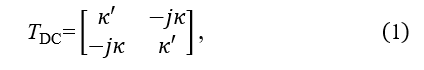
where and are the amplitudes of optical field coupled to the through and cross ports, respectively, and for a lossless DC. Then the optical output powers in the through and cross ports are given as

respectively, where is the power coupling ratio of DC and is the phase given by the arm waveguide [1]. Equations (2) and (3) indicate that crosstalk to through port becomes zero only if in cross state ( ), while crosstalk to cross port vanishes regardless of in through state ( ). In general, the wavelength dependence of is greater than that of , cross port (in through state) offers lower crosstalk than through port (in cross state). In a 1 × N switch composed of cascaded MZIs shown in Figure 1, the number of output ports with low crosstalk is less than half of the total optical output counts.
The conventional cascaded MZI optical switch, however, is not suitable for the hybrid structure because its phase shifters are placed in series. This makes it difficult to fabricate the phase shifter and other waveguide regions with different material. As the output port counts and the number of MZIs with the phase shifter increase, the transmission loss becomes larger since the coupling loss between the waveguides with different materials is accumulated every time passing through the MZI.
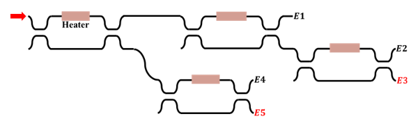
Figure 1: Conventional cascaded MZI optical switch
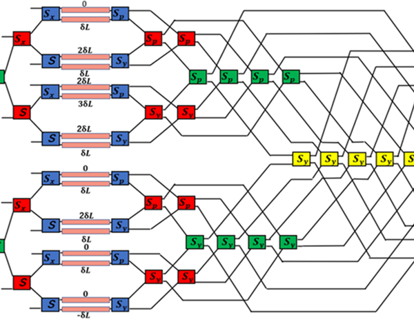
Figure 2: Circuit configuration of 4-stage nested MZI switch with PGCs
In contrast, a nested MZI switch [14-16, 18] is suitable for the hybrid structure because its phase shifters are placed in parallel. It is easy to fabricate the phase shifter and the other waveguide regions separately with different materials, and transmission loss does not increase with the number of output ports.
Figure 2 shows a circuit configuration of the optical switch we examined in this paper. This circuit corresponds to an MZI switch arranged in a nested architecture with four stages [18]. The PGCs indicated in different colors (blue, red, green and yellow) construct the first, second, third and fourth stages, respectively. An inherent symmetry of this circuit configuration makes it easy to increase the number of stages and output port counts [16]. However, the crosstalk characteristics of the nested MZI optical switch with a large number of stages has not been clarified yet.
3. Simulation Method
| Stage
Output |
1st stage | 2nd stage | 3rd stage | 4th stage |
| O1 | T | T | T | T |
| O2 | C | T | T | T |
| O3 | C | C | T | T |
| O4 | T | C | T | T |
| O5 | T | C | C | T |
| O6 | C | C | C | T |
| O7 | C | T | C | T |
| O8 | T | T | C | T |
| O9 | T | T | C | C |
| O10 | C | T | C | C |
| O11 | C | C | C | C |
| O12 | T | C | C | C |
| O13 | T | C | T | C |
| O14 | C | C | T | C |
| O15 | C | T | T | C |
| O16 | T | T | T | C |
We employ PGCs instead of the DCs in all nested MZIs. Figure 3 shows the circuit configurations of the PGCs: a basic element as well as those having the line symmetries with respect to X- or Y-axes and point symmetry. The PGCs in each MZI stages are arranged in mirror symmetry as shown in Figure 2. In order to give an optical phase shift of π, appropriate optical path length differences are set between the arm waveguides connecting the PGCs, as also shown in Figure 2. Table 1 shows the MZI state of each stage for given optical output ports. In Table 1, C denotes that the corresponding MZI stage is in cross state while T does that it is in through state. Table 2 shows the phase settings to route each optical output port, where is that of i-th phase shifter, and and indicate the phase shift of 0 and π, respectively.
Figure 3: Basic PGC element, line-symmetric (with X- or Y-axes) and point-symmetric PGCs MZI state: C = cross, T = through
| Table 2: Phase settings |
| O1 | 0 | 0 | 0 | 0 | 0 | 0 | 0 | 0 | 0 | 0 | 0 | 0 | 0 | 0 | 0 | 0 |
| O2 | 0 | 1 | 1 | 0 | 0 | 1 | 1 | 0 | 0 | 1 | 1 | 0 | 0 | 1 | 1 | 0 |
| O3 | 0 | 1 | 0 | 1 | 1 | 0 | 1 | 0 | 0 | 1 | 0 | 1 | 1 | 0 | 1 | 0 |
| O4 | 0 | 0 | 1 | 1 | 1 | 1 | 0 | 0 | 0 | 0 | 1 | 1 | 1 | 1 | 0 | 0 |
| O5 | 0 | 0 | 1 | 1 | 0 | 0 | 1 | 1 | 1 | 1 | 0 | 0 | 1 | 1 | 0 | 0 |
| O6 | 0 | 1 | 0 | 1 | 0 | 1 | 0 | 1 | 1 | 0 | 1 | 0 | 1 | 0 | 1 | 0 |
| O7 | 0 | 1 | 1 | 0 | 1 | 0 | 0 | 1 | 1 | 0 | 0 | 1 | 0 | 1 | 1 | 0 |
| O8 | 0 | 0 | 0 | 0 | 1 | 1 | 1 | 1 | 1 | 1 | 1 | 1 | 0 | 0 | 0 | 0 |
| O9 | 0 | 0 | 0 | 0 | 1 | 1 | 1 | 1 | 0 | 0 | 0 | 0 | 1 | 1 | 1 | 1 |
| O10 | 0 | 1 | 1 | 0 | 1 | 0 | 0 | 1 | 0 | 1 | 1 | 0 | 1 | 0 | 0 | 1 |
| O11 | 0 | 1 | 0 | 1 | 0 | 1 | 0 | 1 | 0 | 1 | 0 | 1 | 0 | 1 | 0 | 1 |
| O12 | 0 | 0 | 1 | 1 | 0 | 0 | 1 | 1 | 0 | 0 | 1 | 1 | 0 | 0 | 1 | 1 |
| O13 | 0 | 0 | 1 | 1 | 1 | 1 | 0 | 0 | 1 | 1 | 0 | 0 | 0 | 0 | 1 | 1 |
| O14 | 0 | 1 | 0 | 1 | 1 | 0 | 1 | 0 | 1 | 0 | 1 | 0 | 0 | 1 | 0 | 1 |
| O15 | 0 | 1 | 1 | 0 | 0 | 1 | 1 | 0 | 1 | 0 | 0 | 1 | 1 | 0 | 0 | 1 |
| O16 | 0 | 0 | 0 | 0 | 0 | 0 | 0 | 0 | 1 | 1 | 1 | 1 | 1 | 1 | 1 | 1 |
| Table 1: MZI states |
We calculated the optical transmittance of the nested MZI to each output port by the same method as the previous study [16]. The circuit parameters used in this study was also the same as those given previously. The power coupling ratio of the PGCs was designed to be 50 % (3 dB) at 1550 nm, the center wavelength of operating range. The parameters of the PGC are as follows: coupling lengths = 20 μm and = 10 μm, delay line length = 0.086 μm, and optical path length difference = 0.4 μm.
The optical output field of a single-stage MZI switch with PGCs (configuration and ) is given as
where and indicate output fields in through and cross ports, respectively. In equation (4),
indicate transfer matrix of , the arm waveguides, and , respectively [16]. Here, and indicate transfer functions of through and cross ports in the PGC, respectively. is a complex conjugate of the transfer function , and is a phase difference between the arm waveguides connecting the PGCs. We simulated the optical output power of a multi-stage MZI switch with PGCs by multiplying these transfer matrices in appropriate order.
4. Results and Discussion
4.1. Results
Figures 4(a)−4(p) show the calculated optical transmittance of the switch we propose when the optical signal is routed to output ports O1−O16, respectively. Here, the transmittance is defined as the ratio of the optical output power to the optical input power. Wavelength dependence was computed in increments of 0.1 nm.
In Figure 4(a) where the optical input signal is routed to O1, crosstalks to unrouted ports of O2, O4, O8 and O16 are the same and less than −30 dB in 200 nm wavelength range from 1450 to 1650 nm. Crosstalks to O3, O5, O7, O9, O13 and O15 are lower than −60 dB, while those to O6, O10, O12 and O14 are below −100 dB. In particular, O11 has quite low crosstalk below −130 dB. In all O2−O16, crosstalks are dropped at two wavelengths of 1490 and 1630nm, where the PGCs create the phase that exactly cancels the wavelength dependence of the arm waveguides.
However, in Figure 4(b) where the optical signal is directed to O2, crosstalk to O1 increases and becomes higher than −20 dB as the signal wavelength is away from a center wavelength. This is because the power coupling ratio of the PGC deviates from 50 % (3 dB) due to its wavelength dependence. Crosstalks to O3, O7 and O15 are identical and less than −30 dB within the 200 nm wavelength range around 1550 nm, while those to O4, O8 and O16 are lower than −40 dB. Other ports have much lower crosstalks below −60 dB.
When the optical path is set toward O4, O8 and O16, respectively, O1 has high crosstalk as same as the output is set at O2. Crosstalk to O1 is a little bit low but higher than −20 dB when the optical input signal is directed to O3, O5, O7, O9, O13 and O15, respectively. When the optical signal is routed to O6, O10, O12 and O14, respectively, crosstalk to O1 is identical and also exceeds −20 dB. In the case that the routed port is O11, it remains higher than −20 dB within the wavelength range of 1550 ± 100 nm. These results indicate that we should avoid to use O1 as the output port of the nested MZI optical switch.
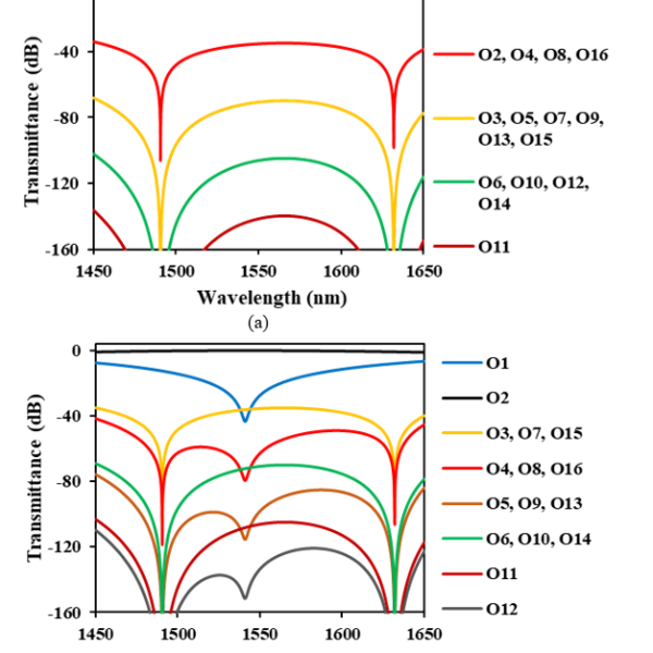
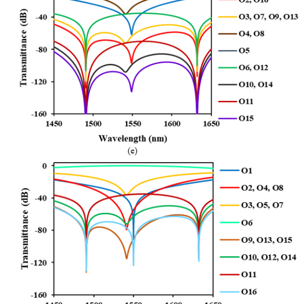
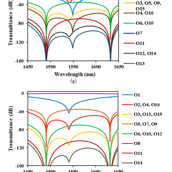
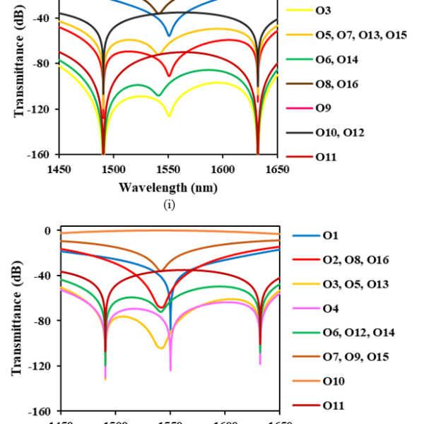
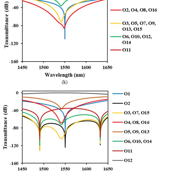
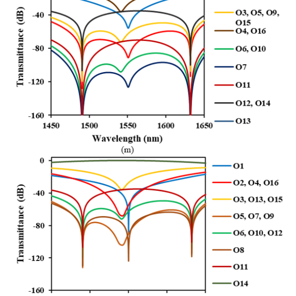
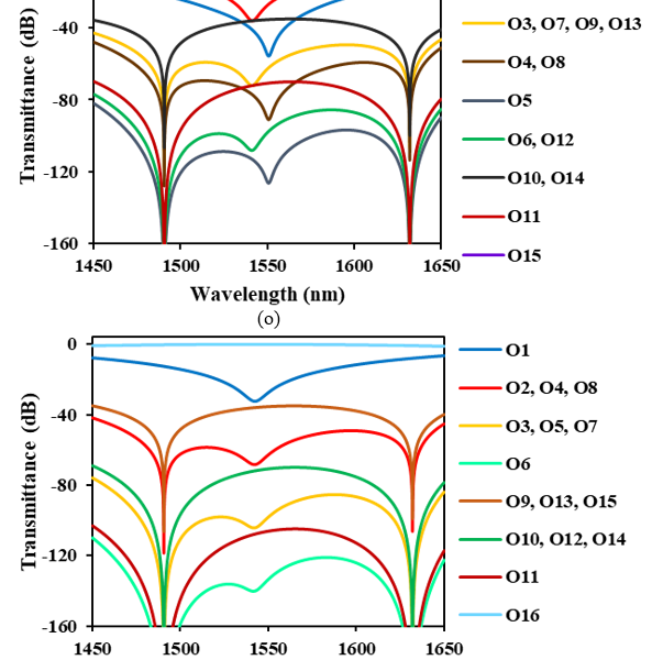
Figure 4: Transmittance of 4-stage nested MZI switch with PGCs when the optical path is set toward O1−O16 (a) O1 (b) O2 (c) O3 (d) O4 (e) O5 (f) O6 (g) O7 (h) O8 (i) O9 (j) O10 (k) O11 (l) O12 (m) O13 (n) O14 (o) O15 (p) O16
We examined the crosstalk characteristics shown in Figures 4(a)−4(p), and found that cross talks to un routed ports are suppressed to −40 dB or less over the wavelength band of 200 nm ranging from 1450 to 1650 nm when we choose only O3, O5, O7, O9, O13 and O15 as the output port of the nested MZI optical switch. In Figure 4(c) where the optical input signal is routed to O3, cross talks to O5, O7, O13 and O15 are identical and less than −40 dB. O9 has much lower crosstalk below −80 dB. When we avoid to use other ports as output, cross talks to un routed ports (O5, O7, O9, O13 and O15) never exceed −40 dB. In Figures 4(e), 4(g), 4(i), 4(m) and 4(o), cross talks remain lower than −40 dB when the optical signal is routed to O5, O7, O9, O13 and O15, respectively.
4.2. Discussion
The crosstalk characteristics of 16 ports shown in Figures 4(a)−4(p) is classified into 5 groups. One is O1, second is O2, O4, O8 and O16, third is O3, O5, O7, O9, O13 and O15, forth is O6, O10, O12 and O14, and the last is O11. Each group has the same number of the MZI states (cross or through) as shown in Table 1. This means that the port settings in the same group have two or more different MZI states among four stages each other. For example, the port settings in the third group (O3, O5, O7, O9, O13 and O15) have two cross states and two through states among four MZI stages. O3 has the MZI states of CCTT, where C or T denotes each MZI state of four stages as shown in Table 1. This state differs in two stages to those of O5 (TCCT), O7 (CTCT), O13 (TCTC) and O15 (CTTC), while in all four stages to O9 (TTCC). Thus, when the optical path is set toward O3, crosstalks to O5, O7, O13 and O15 are blocked in two MZI stages where one is in cross state and the other is in through state, respectively, and that to O9 in four MZI stages where two are in cross state and the other two are in through state. Crosstalks to unrouted ports are blocked similarly when the optical signal is routed to O5, O7, O9, O13 and O15, respectively. This is why the lower crosstalk is given when we choose only O3, O5, O7, O9, O13 and O15 as the output ports of the nested MZI optical switch.
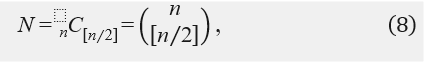
Following the analysis above, we can deduce how many output ports in multi-stage nested MZI switch has low crosstalk. We should choose the port settings which have the same number of the MZI states (cross or through) and equalize the cross and through states. Then the number of output ports with low crosstalk in an -stage switch ( ) is given as
where is a floor function. In the previous study [16], it has been shown that a 2-stage nested MZI switch has two ports with low crosstalk among four output ports. A 3-stage nested MZI optical switch gives three ports with low crosstalk in eight output ports. This study shows that 4-stage nested MZI switch has six ports with low crosstalk in 16 output ports. Equation (8) agrees with these results, and indicates that 5-stage nested MZI switch must have ten ports with low crosstalk in 32 output ports. Figure 5 shows the required number of stages for given output port counts with low crosstalk. The ratio of to is less than 50 % and decreases as increases. However, the conventional MZI optical switch commonly employ two cascaded MZIs per output port to suppress crosstalk sufficiently [16-18]. In that case the ratio is around 50 % for the conventional cascaded MZI switch. Although the nested MZI switch has somewhat smaller ratio of the output ports with low crosstalk, it has advantages that its phase shifters are placed in parallel and gives a shorter circuit length than the cascaded MZI optical switch.
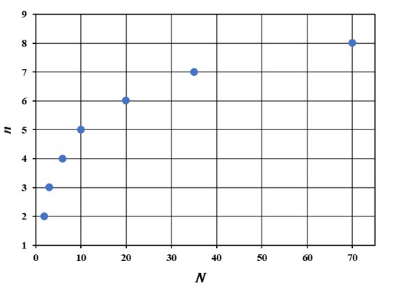
Figure 5: Required number of stages for given output port counts with low crosstalk
Recently, a new concept was demonstrated that effectively reduces the wavelength dependence of an MZI switch [19]. This technique employs no PGCs but arm waveguides with different waveguide widths in each cascaded MZI. It is a future work whether this technique is possible to apply to the nested MZI switch with arrayed arm waveguides.
5. Conclusion
We examined the crosstalk characteristics of a 4-stage nested MZI optical switch with PGCs. It was confirmed that crosstalk is lower than −40 dB over a wavelength band of as wide as 200 nm ranging from 1450 to 1650 nm in six output ports of the 4-stage switch. We showed that crosstalks to these six ports are blocked in two MZI stages where one is in cross state and the other is in through state, respectively. Based on the results, we deduced the required number of stages for given output port counts with low crosstalk in multi-stage nested MZI switch. It is possible to construct 1 × 10, 1 × 20, 1 × 35 optical switches with 5, 6, 7-stages, respectively, and output port count reaches 70 in 8-stage nested MZI switch.
Conflict of Interest
We declare no conflict of interest.
Acknowledgment
This work was partly supported by JSPS KAKENHI Grant Number JP18K04286.
- N. Takato, K. Jinguji, M. Yasu, H. Toba, and M. Kawachi, “Silica-based single-mode waveguides on silicon and their application to guided-wave optical interferometers,” Journal of Lightwave Technology, 6(6), 1003-1010, 1988, doi: 10.1109/50.4091.
- S. Sohma, S. Mino, T. Watanabe, M. Ishii, T. Shibata, and H. Takahashi, “Solid-state optical switches using planar lightwave circuit and IC-on-PLC technologies,” Proceedings of SPIE, 5625, 767-775, 2004, doi: 10.1117/12.579684.
- H. Takahashi, T. Watanabe, T. Goh, S. Sohma, and T. Takahashi, “PLC optical switch that enhances the optical communication network,” NTT Technical Review, 3(7), 17-21, 2005.
- C. R. Doerr and K. Okamoto, “Advances in silica planar lightwave circuits,” Journal of Lightwave Technology, 24(12), 4763-4789, 2006, doi: 10.1109/JLT.2006.885255.
- T. Watanabe, K. Suzuki, T. Goh, K. Hattori, A. Mori, T. Takahashi, T. Sakamoto, K. Morita, S. Sohma, and S. Kamei, “Compact PLC-based transponder aggregator for colorless and directionless ROADM,” Technical Digest of 2011 Optical Fiber Communication Conference/National Fiber Optic Engineers Conference (OFC/NFOEC 2011), paper OTuD3, 2011, doi: 10.1364/OFC.2011.OTuD3.
- K. Sato, H. Hasegawa, T. Niwa, and T. Watanabe, “A large-scale wavelength routing optical switch for data center networks,” IEEE Communications Magazine, 51(9), 46-52, 2013, doi: 10.1109/MCOM.2013.6588649.
- N. Farrington, A. Forencich, G. Porter, P.-C. Sun, J. E. Ford, Y. Fainman, G. C. Papen, and A. Vahdat, “A multiport microsecond optical circuit switch for data center networking,” IEEE Photonics Technology Letters, 25(16), 1589-1592, 2013, doi: 10.1109/LPT.2013.2270462.
- Q. Cheng, M. Bahadori, M. Glick, S. Rumley, and K. Bergman, “Recent advances in optical technologies for data centers: a review,” Optica, 5(11), 1354-1370, 2018, doi: 10.1364/OPTICA.5.001354.
- S. Katayose, Y. Hashizume, and M. Itoh, “Fabrication and demonstration of 1 × 8 silicon-silica multi-chip switch based on optical phased array,” Japanese Journal of Applied Physics, 55, 08RB01, 2016, doi: 10.7567/JJAP.55.08RB01.
- O. Moriwaki and K. Suzuki, “Fast switching of 84 s for silica-based PLC switch,” Technical Digest of 2020 Optical Fiber Communication Conference (OFC 2020), paper Th3B.5, 2020, doi: 10.1364/OFC.2020.Th3B.5.
- K. Hattori, M. Fukui, M. Jinno, M. Oguma, and K. Oguchi, “PLC-based optical add/drop switch with automatic level control,” Journal of Lightwave Technology, 17(12), 2562-2571, 1999, doi: 10.1109/50.809678.
- H. Takahashi, T. Goh, T. Shibata, M. Okuno, Y. Hibino, and T. Watanabe, “High performance 8-arrayed 1 × 8 optical switch based on planar lightwave circuit for photonic networks,” Proceedings of 28th European Conference on Optical Communication (ECOC 2002), paper 4.2.6, 2002.
- T. Watanabe, Y. Hashizume, and H. Takahashi, “Double-branched 1×29 silica-based PLC switch with low loss and low power consumption,” Technical Digest of 17th Microoptics Conference (MOC 2011), paper J-2, 2011.
- K. Suzuki, T. Mizuno, M. Oguma, T. Shibata, H. Takahashi, Y. Hibino, and A. Himeno, “Low loss fully reconfigurable wavelength-selective optical 1 × N switch based on transversal filter configuration using silica-based planar lightwave circuit,” IEEE Photonics Technology Letters, 16(6), 1480-1482, 2004, doi: 10.1109/LPT.2004.827419.
- T. Watanabe, K. Tasaki, T. Nagayama, and S. Fukushima, “Nested Mach-Zehnder interferometer optical switch with low crosstalk,” Technical Digest of 24th Microoptics Conference (MOC 2019), paper P-69, 2019, doi: 10.23919/MOC46630.2019.
- K. Tasaki, M. Tokumaru, T. Watanabe, T. Nagayama, and S. Fukushima, “Nested Mach-Zehnder interferometer optical switch with phase generating couplers,” Japanese Journal of Applied Physics, 59, SOOB04, 2020, doi: 10.35848/1347-4065/ab8f09.
- T. Mizuno, H. Takahashi, T. Kitoh, M. Oguma, T. Kominato, and T. Shibata, “Mach–Zehnder interferometer switch with a high extinction ratio over a wide wavelength range,” Optics Letters, 30(3), 251-253, 2005, doi: 10.1364/OL.30.000251.
- M. Kawasako, T. Watanabe, T. Nagayama, and S. Fukushima, “4-stage Mach-Zehnder interferometer optical switch with phase generating couplers,” Technical Digest of 26th Microoptics Conference (MOC 2021), paper P-40, 2021, doi: 10.23919/MOC52031.2021.
- T. Goh, K. Yamaguchi, and A. Yanagihara, “Multiband optical switch technology,” Technical Digest of 2022 Optical Fiber Communication Conference (OFC 2022), paper W4B.1, 2022, doi: 10.1364/OFC.2022.W4B.1.
No related articles were found.