Characteristics of Crystal Defects due to the Inverse Piezoelectric Effect in Aluminum Gallium Nitride / Gallium Nitride High Electron Mobility Transistors

Adv. Sci. Technol. Eng. Syst. J. 10(3), 9–14 (2025);
 DOI: 10.25046/aj100302
Gallium nitride (GaN) is expected to be used as a material for power semiconductor devices. However, it is crucial to focus on the dielectric properties of GaN. In this study, we investigated the transient response of the drain current during high-frequency application after intentionally maintaining the current collapse in the AlGaN/GaN high electron mobility transistors. The experiment observed a long-term current recovery process of approximately 50 s and showed a temperature dependence that was opposite to the steady state at high temperatures. In addition, by changing the duration of the current collapse, it was suggested that the electron trapping in the crystal defects, generated by the strain expansion due to the inverse piezoelectric effect, was promoted by maintaining the current collapse. Furthermore, we analyzed the activation energy calculated from the current value using the temperature dependence of the transient response. The change in the activation energy from approximately 0.6 to 1.0 eV clarified the behavior of electron trapping and de-trapping, including the effect of the inverse piezoelectric effect. The experimental results suggested the existence of recoverable crystal defects caused by the inverse piezoelectric effect.
1. Introduction
In recent years, the performance of Si-based semiconductor devices has reached its limit; therefore, dielectric materials with large bandgaps have been used. Gallium nitride (GaN) has a bandgap energy of 3.4 eV and is expected to be used in power semiconductor devices [1], [2]. AlGaN/GaN high-electron-mobility transistors (HEMTs) can be implemented by heterojunction of aluminum gallium nitride (AlGaN) and GaN [3], [4]. The spontaneous polarization of AlGaN and GaN, as well as the piezoelectric polarization of the junction due to lattice mismatch, results in the accumulation of positive fixed charges at the bottom of the AlGaN layer and negative fixed charges at the top of the GaN layer. The greater number of positive fixed charges on the AlGaN side results in a concentration of electrons at the top of the GaN layer, thereby compensating for this imbalance and resulting in the formation of a two-dimensional electron gas (2DEG) [5], [6]. When a large reverse voltage is applied to the gate electrode, the inverse piezoelectric effect amplifies the tensile stress caused by the existing polarization, resulting in the expansion of strain and the generation of crystal defects [7]–[12]. In piezoelectric materials, the direct piezoelectric effect causes polarization due to strain, while the inverse piezoelectric effect causes the distortion due to an electric field. In a GaN-HEMT, the former contributes to the formation of a 2DEG, and the latter results in performance degradation.
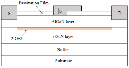
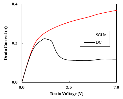
In addition, GaN devices have numerous crystal defects that trap electrons, resulting in the expansion of the depletion layer and a decrease in the drain current [13]–[15]. Furthermore, electrons are trapped on the surface of the AlGaN layer due to the concentration of the electric field at the edge of the gate electrode in the direction of the drain electrode [15]–[17]. This problem, known as the current collapse phenomenon, results in performance degradation. A field-plate structure for the gate electrode is one way to suppress current collapse [18], [19]. This structure prevented electric field concentration. Additionally, the application of a high frequency to the gate electrode, which exceeds the time constant of the crystal defects, has been demonstrated to suppress electron trapping [20], [21]. Figure 1 shows a schematic cross-section of the AlGaN/GaN HEMT, and Figure 2 shows the I-V characteristics when a high frequency (5 GHz) and DC are applied.
In this study, we investigated the transient response of the drain current during high-frequency applications after intentionally maintaining the current collapse in an AlGaN/GaN HEMT. The experiment revealed a long-term current recovery process and showed a temperature dependence opposite to that of the steady state at high temperatures. Additionally, by changing the duration of the current collapse, the duration affected the current recovery rate. Furthermore, the change in activation energy calculated from the current value was analyzed. The experimental results suggested the occurrence of recoverable strain owing to the inverse piezoelectric effect. The present study investigated the influence of the inverse piezoelectric effect on a GaN-HEMT using a different method than previous studies [11], [12]. This method involved switching between promoting and suppressing the current collapse by changing the frequency, and calculating the change in activation energy from the difference in current values during transient response.
2. Experimental Methods
2.1. Measuring I-V characteristics after maintaining the current collapse
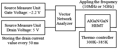
In this experiment, 10 MHz was applied to the AlGaN/GaN HEMT (CGH40025F, CREE) in the operating state for a certain period. Following 5 s in the nonoperating state, we measured I-V characteristics when applying 5 GHz at room temperature. Time of the 10MHz operation was modulated from 100 s to 250 s. The gate voltage was set to –2.2 V. The drain voltage was set to 5 V for 10 MHz operation, and was swept from 0 V to 8 V in 0.1 V increments for I-V characteristic measurements. Frequency was applied to the gate electrode using a vector network analyzer (MS4644B, Anritsu). Switching between states was achieved by taking advantage of the fact that the current collapse could not be suppressed at 10 MHz but could be suppressed at 5 GHz.
2.2. Measuring drain current transient response after maintaining the current collapse
In this experiment, 10 MHz was applied to the AlGaN/GaN HEMT in the operating state for 150 s. Following 5 s in the nonoperating state, 5 GHz was again applied in the operating state for 150 s. Simultaneously, we measured the transient response of the drain current when 5 GHz was applied, using a source-measure unit (GS610, YOKOGAWA).
The gate voltage was set to –2.2 V and the drain voltage to 5 V, and measurements were performed from 300 K to 385 K. To eliminate the influence of the previous measurement, the device was operated at 5 GHz with a drain voltage of 10 V for 5 s before and after each measurement.
Additionally, measurements were conducted from 340 K to 385 K while modulating the time of the 10 MHz operation from 100 s to 250 s. Each measurement was performed after the temperature on the surface of the device package had stabilized. Figure 3 shows the experimental system used in this experiment.
3. Results and Discussion
3.1. I-V characteristics after maintaining the current collapse
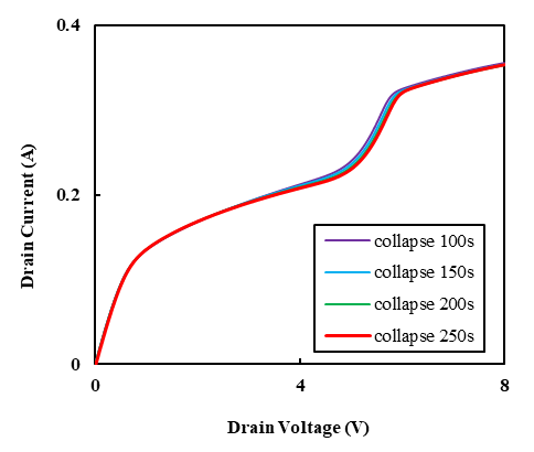
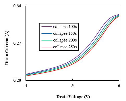
Figure 4 shows the I-V characteristics after maintaining the current collapse for each duration. An enlarged view of the range from 4 V to 6 V is shown in Figure 5. The maintenance of the current collapse resulted in the occurrence of kink effect, the kink effect became stronger depending on the maintenance time. A decrease in drain current was observed at a bias where 2DEG formation and electron de-trapping were inadequate.
3.2. Drain current transient response after maintaining the current collapse
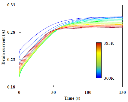
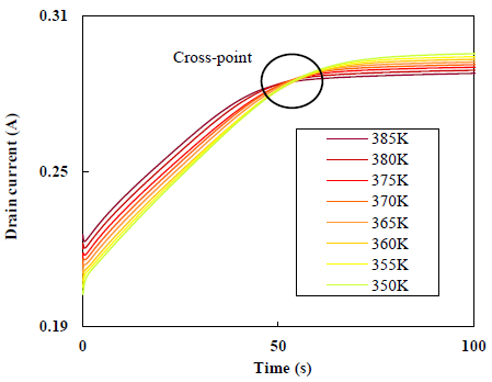
The temperature dependence of the drain-current transient response after the current collapse was maintained is shown in Figure 6. In the steady state, the higher the temperature, the lower the current. This was attributed to the inhibition of carrier transport caused by phonon scattering [22], [23]. However, in the transient region, the opposite of the steady state was observed at temperatures above approximately 340 K. Figure 7 shows the transient response above 350 K, where a reversal of the characteristics can be observed. Waveform crossings caused by the reversal were confirmed. The maintenance of the current collapse resulted in a limited number of carriers in the 2DEG following the resumption of operations. Therefore, the impact of increasing the number of thermal carriers and accelerating electrons owing to thermal energy was more pronounced than the inhibition of carrier transport owing to phonon scattering.
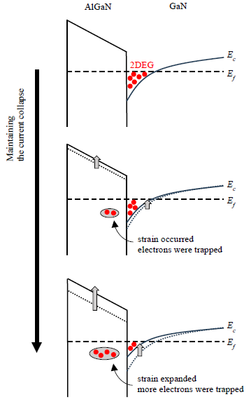
A high frequency was applied during the transient response measurement, thereby prompting the de-trapping of electrons from the crystal defects. However, because the transient response was long, there was an effect other than simple electron de-trapping. Therefore, we focus on the strain induced by the inverse piezoelectric effect. The inverse piezoelectric effect, caused by the electric field, results in strain and results in the formation of crystal defects [7], [8]. Assuming that the inverse piezoelectric effect caused by the gate voltage generated defects in the AlGaN crystal while maintaining the current collapse, electrons were trapped in these defects. Although the polarization due to the inverse piezoelectric effect was unable to respond to a high frequency, the restoration of strain required a temporal span, resulting in current degradation.
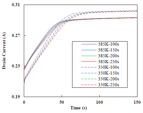
Figure 8 shows the relationship between the current collapse maintenance time and drain current transient response at 350 and 385 K. The longer the duration of the current collapse, the slower the current recovery. As the duration of the current collapse increases, the strain induced by the inverse piezoelectric effect also increases. Figure 9 shows a band diagram representing how the strain induced by the inverse piezoelectric effect expands and traps electrons. As the electron trapping for stain progressed, the band shifted upward and the triangular potential well became shallower.
3.3. Analysis of activation energy
Next, the activation energy was calculated from the current values above 350 K. For current values above 355 K, the difference value was calculated based on the current value at 350 K. Specifically, the current value at the absolute temperature T was defined as IT, and the difference from the standard value was defined as ΔIT, and the following calculation was performed at each temperature.
ΔI355 = I355 – I350 (1)
ΔI360 = I360 – I350 (2)
⁝
ΔI385 = I385 – I350 (7)
The activation energy ΔE was calculated from ΔIT and the following Arrhenius equation.
ΔIT = A exp( –ΔE / kT ) (8)
Here, A is a constant, and k is Boltzmann’s constant. ΔE was calculated for each time of the transient response within the range where (8) was accurate. As an example of ΔE calculation, Figure 10 shows an Arrhenius plot for a transient response time of 1 s at the current collapse time of 250 s. In this example, a precise Arrhenius plot was obtained with a coefficient of determination of 0.975.
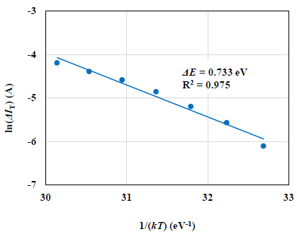
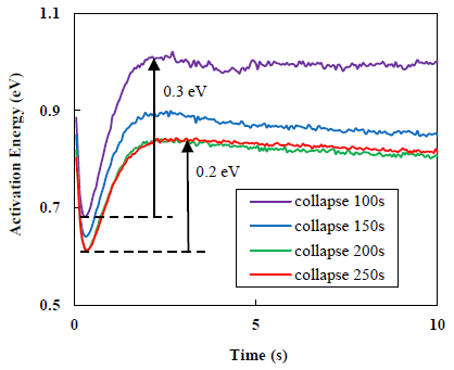
Figure 11 shows the change in activation energy for each duration of the current collapse. The energy value dropped sharply between 0.3 and 0.4 s, then rose and stabilized. The current collapse was maintained, thereby decreasing the activation energy immediately following the resumption of operation, owing to the de-trapping of electrons. Subsequently, as electron trapping progressed, the activation energy increased. When trapping and de-trapping reached equilibrium, the activation energy stabilized. The amount of the increase from the lower limit of the energy value to the point of stabilization was approximately 0.3 eV for a collapse time of 100 s and 0.2 eV for 250 s. When the duration of the current collapse was long, many of the crystal defects were filled with electrons; therefore, de-trapping progressed more easily than new trapping, resulting in only a small increase in activation energy. The strain induced by the inverse piezoelectric effect increased the timescale of the activation energy change. Furthermore, as the effect reached its saturation point, there was almost no difference between the 200 s and 250 s cases.
4. Conclusion
In this study, we investigated the transient response of the drain current during high-frequency applications by controlling the promotion and suppression of the current collapse by switching the frequency applied to the gate electrode in a GaN-HEMT. In the experiment, a long-term current recovery process was observed, suggesting that electron trapping in the crystal defects, generated by strain expansion owing to the inverse piezoelectric effect, was promoted by maintaining the current collapse. The activation energy was calculated using the temperature dependence, which was opposite to the steady state at high temperatures. The change in the obtained activation energy clarified the electron trapping and de-trapping behavior, including the inverse piezoelectric effect. Furthermore, extending the duration of the current collapse saturated the effect. The experimental results suggested the existence of recoverable crystal defects caused by the inverse piezoelectric effect. A critical focus in the research community is to emphasize the dielectric properties of GaN, a wide-bandgap material, in order to enhance our understanding of its unique characteristics and applications.
Conflict of Interest
The authors declare no conflict of interest.
Acknowledgment
The authors are grateful to the Chukyo University Research Foundation for financial assistance with this study.
We would like to thank Editage (www.editage.jp) for English language editing.
- J. Millán, P. Godignon, X. Perpiñà, A. Pérez-Tomás, J. Rebollo, “A survey of wide bandgap power semiconductor devices,” in IEEE Transactions on Power Electronics, 29(5), 2155–2163, 2014, doi:10.1109/TPEL.2013.2268900.
- E.A. Jones, F.F. Wang, D. Costinett, “Review of commercial GaN power devices and GaN-based converter design challenges,” in IEEE Journal of Emerging and Selected Topics in Power Electronics, 4(3), 707–719, 2016, doi:10.1109/JESTPE.2016.2582685.
- N.A. Torkhov, L.I. Babak, A.A. Kokolov, “The influence of AlGaN/GaN heteroepitaxial structure fractal geometry on size effects in microwave characteristics of AlGaN/GaN HEMTs,” Symmetry, 11(12), 1495, 2019, doi:10.3390/sym11121495.
- S. Ghosh, A.M. Hinz, M. Frentrup, S. Alam, D.J. Wallis, R.A. Oliver, “Design of step-graded AlGaN buffers for GaN-on-Si heterostructures grown by MOCVD,” Semiconductor Science and Technology, 38(4), 044001, 2023, doi:10.1088/1361-6641/acb9b6.
- K. Osipov, I. Ostermay, M. Bodduluri, F. Brunner, G. Tränkle, J. Würfl, “Local 2DEG density control in heterostructures of piezoelectric materials and its application in GaN HEMT fabrication technology,” in IEEE Transactions on Electron Devices, 65(8), 3176–3184, 2018, doi:10.1109/TED.2018.2850010.
- J. He, W.C. Cheng, Q. Wang, K. Cheng, H. Yu, Y. Chai, “Recent advances in GaN‐based power HEMT devices,” Advanced electronic materials, 7(4), 2001045, 2021, doi:10.1002/aelm.202001045.
- J. Joh, L. Xia, J.A. del Alamo, “Gate current degradation mechanisms of GaN high electron mobility transistors,” 2007 IEEE International ElectronDevices Meeting, Washington, DC, USA, 385–388, 2007, doi:10.1109/IEDM.2007.4418953.
- U. Chowdhury, J.L. Jimenez, C. Lee, E. Beam, P. Saunier, T. Balistreri, S.Y. Park, T. Lee, J. Wang, M.J. Kim, et al. “TEM observation of crack- and pit-shaped defects in electrically degraded GaN HEMTs,” in IEEE Electron Device Letters, 29(10), 1098–1100, 2008, doi:10.1109/LED.2008.2003073.
- L. Shi, S. Feng, Y. Zhang, B. Shi and K. Liu, “Variation of dominant degradation mechanism in AlGaN barrier layer with different voltage stress on the gate of AlGaN/GaN high electron mobility transistors,” in IEEE Electron Device Letters, 36(4), 321–323, 2015, doi:10.1109/LED.2015.2399774.
- K. Ahmeda, B. Ubochi, B. Benbakhti, S.J. Duffy, A. Soltani, W.D. Zhang, K. Kalna, “Role of self-heating and polarization in AlGaN/GaN-based heterostructures,” in IEEE Access, 5, 20946–20952, 2017, doi:10.1109/ACCESS.2017.2755984.
- H. Shiomi, A. Ueda, T. Tohei, Y Imai, T. Hamachi, K. Sumitani, S. Kimura, Y. Ando, T. Hashizume, A. Sakai, “Analysis of inverse-piezoelectric-effect-induced lattice deformation in AlGaN/GaN high-electron-mobility transistors by time-resolved synchrotron radiation nanobeam X-ray diffraction,” Applied Physics Express, 14(9), 095502, 2021, doi:10.35848/1882-0786/ac1ee4.
- Y. Zhang, L. Zhou, J.-F. Mao, “Inverse piezoelectric and trap effects with temperature dependence in AlGaN/GaN HEMTs under narrowband microwave pulses,” in IEEE Transactions on Electromagnetic Compatibility, 6(53), 794–803, 2023, doi:10.1109/TEMC.2023.3237318.
- S. Mukherjee, E.E. Patrick, M.E. Law, “Simulation of deep-level trap distributions in AlGaN/GaN HEMTs and its influence on transient analysis of drain current,” ECS Journal of Solid State Science and Technology, 6(11), S3093, 2017, doi:10.1149/2.0211711jss.
- R. Ye, X. Cai, C. Du, H. Liu, Y. Zhang, X. Duan, J. Zhu, “An overview on analyses and suppression methods of trapping effects in AlGaN/GaN HEMTs,” in IEEE Access, 10, 21759–21773, 2022, doi:10.1109/ACCESS.2021.3139443.
- M. Meneghini, A. Tajalli, P. Moens, A. Banerjee, E. Zanoni, G. Meneghesso, “Trapping phenomena and degradation mechanisms in GaN-based power HEMTs,” Materials Science in Semiconductor Processing, 78, 118–126, 2018, doi:10.1016/j.mssp.2017.10.009.
- I. Rossetto, M. Meneghini, A. Tajalli, S. Dalcanale, C. De Santi, P. Moens, A. Banerjee, E. Zanoni, G. Meneghesso, “Evidence of hot-electron effects during hard switching of AlGaN/GaN HEMTs,” in IEEE Transactions on Electron Devices, 64(9), 3734–3739, 2017, doi:10.1109/TED.2017.2728785.
- T. Mizutani, Y. Ohno, M. Akita, S. Kishimoto, K. Maezawa, “A study on current collapse in AlGaN/GaN HEMTs induced by bias stress,” in IEEE Transactions on Electron Devices, 50(10), 2015–2020, 2003, doi:10.1109/TED.2003.816549.
- W. Saito, T. Nitta, Y. Kakiuchi, Y. Saito, K. Tsuda, I. Omura, M. Yamaguchi, “Suppression of dynamic on-resistance increase and gate charge measurements in high-voltage GaN-HEMTs with optimized field-plate structure,” in IEEE Transactions on Electron Devices, 54(8), 1825–1830, 2007, doi:10.1109/TED.2007.901150.
- H. Huang, Y.C. Liang, G.S. Samudra, T.-F. Chang, C.-F. Huang, “Effects of gate field plates on the surface state related current collapse in AlGaN/GaN HEMTs,” in IEEE Transactions on Power Electronics, 29(5), 2164–2173, 2014, doi:10.1109/TPEL.2013.2288644.
- H. Taguchi, K. Akahori, T. Shimazu, H. Tanabe, “Analysis of drain current transient response of gate pulse voltage in AlGaN / GaN High electron mobility transistors,” Advances in Science, Technology and Engineering Systems Journal, 3(5), 216–219, 2018, doi:10.25046/aj030526.
- Y. Shimizu, A. Fujiwara, H. Hayashi, S. Sano, K. Hirana, H. Taguchi, “Methodology for evaluating 2DEG carrier behavior in high-frequency bands in AlGaN/GaN HEMTs,” TENCON 2023 – 2023 IEEE Region 10 Conference (TENCON), Chiang Mai, Thailand, 570–574, 2023, doi:10.1109/TENCON58879.2023.10322353.
- C. Wang, Y. Xu, X. Yu, C. Ren, Z. Wang, H. Lu, T. Chen, B. Zhang, R. Xu, “An electrothermal model for empirical large- signal modeling of AlGaN/GaN HEMTs including self-heating and ambient temperature effects,” in IEEE Transactions on Microwave Theory and Techniques, 62(12), 2878–2887, 2014, doi:10.1109/TMTT.2014.2364821.
- L. Mitterhuber, R. Hammer, T. Dengg, J. Spitaler, “Thermal characterization and modelling of AlGaN-GaN multilayer structures for HEMT applications,” Energies, 13(9), 2363, 2020, doi:10.3390/en13092363.