On-Chip Testing Schemes of Through-Silicon-Vias (TSVs) in 3D Stacked ICs

Adv. Sci. Technol. Eng. Syst. J. 2(3), 1260–1265 (2017);
 DOI: 10.25046/aj0203159
This paper presents on-chip testing structures to characterize and detect faulty Through Silicon Vias (TSVs) in 3D ICs technology. 3D Gunning Transceiver Logic (GTL) I/O testing is proposed to characterize the performance of 3D TSVs in high speed applications. The GTL testing circuit will fire different data patterns at different frequencies to characterize the transient performance of TSVs. In addition, Different testing schemes based on an oscillation ring testing methodology are proposed to detect TSVs faults such as stuck-at, open, slope and delay degradation, and severe crosstalk TSVs coupling. A parallel ring-based oscillator test structure is proposed and simulated based on a high performance fully tunable electrical circuit pi-model where a single and coupled TSVs with ground-signal-ground (GSG) and ground-signal-signal-ground (GSSG) 3D vias configurations are used as a test vehicle for 3D interconnect characterization and test. Simulation results are presented using the Keysight/Agilent Advance Design System (ADS) and a standard 0.25 µm CMOS process.
1. Introduction
With deep sub-micron silicon processing technology, it becomes more difficult for integrated circuits to achieve higher integration through the scaling down of the transistor feature size. 3D ICs technology stacks multiple dies together and connects them using Through-Silicon Vias (TSVs), which become a promising technology to provide a low cost and high efficient way to increase integration for modern systems [1-2]. However, there are some problems associated with this technology. One of the most important issues is the compound yield loss due to die stacking and TSV failures, which might occur either in the fabrication of the TSV themselves, in the bonding of the TSVs to the next layer, or during the life time of the 3D stack. Thus, to guarantee the stacking yield, the interconnections (TSVs) reliability must be tested. Common TSV defects in this emerging technology can be caused by TSV shorts, opens, delay faults [3], crosstalk induced-delay faults and glitches [4-7].
To insure a low probability of 3D IC failure, integrating embedded test structures in 3D stacked ICs becomes a more attractive solution to avoid traditional probe testing, which becomes an infeasible approach to validate inaccessible nodes after stacking. The embedded test circuits can be integrated during the fabrication process to test a group of TSVs or each TSV individually for different possible defects in the die before stacking. In addition, they can be used to characterize the TSV’s signal integrity effects and the impact of TSVs on the 3D circuit performance after fabrication. The results of these test circuits can then be read out off-chip for post processing. In this paper, A 3D Gunning Transceiver Logic (GTL) I/O testing is proposed to characterize signal integrity of TSVs. Additionally, an oscillation ring (OR) 3D test methodology with different circuits testing schemes, based on our work [8], are presented to detect TSVs failure induced by TSVs shorts, opens, delay faults and crosstalk coupling.
2. An Equivalent Electrical Circuit For TSVs
The paper is organized as follows: a high performance TSV electrical pi-model, which can be used as DUT for 3D TSV testing, is discussed in Section 2. Section 3 discusses the 3D GTL I/O testing to evaluate TSV performance. Section 4 proposes the ring-based oscillation testing schemes to detect TSVs failures and their induced 3D performance degradation. Section 5 concludes the paper.
To test and study the effects of TSVs on 3D circuit performance, a high frequency electrical pi-model, commonly used in literature [9-11], is applied for TSV test and characterization, which is extracted from physical configurations of a common TSV structure. Ground-signal-ground (GSG) and ground-signal-signal-ground (GSSG) vias configurations are used to test single and coupled TSVs for different 3D routing topologies. By leveraging these fully parametric TSV models, different TSV designs can be explored to study the impact of TSVs on the 3D performance. In addition, changing the model parameters gives more insight about how these parameters such as induced resistance and capacitance of TSVs affect the 3D circuit. Figure 1(a) shows a schematic drawing of the high frequency equivalent circuit model of a GSG via configuration [12].
The electrical model of the TSV is expressed as an inductor (Lvia) and a resistor (Rvia), while the capacitive coupling between the vias is modeled as coupling capacitors (Cvia_ox, Cox, and Csil). The parameter Cvia_ox denotes the capacitance of the thin oxide layer surrounding the via barrel, and Cox denotes the capacitance of the oxide layer on the silicon surface and the fringing field between the vias. The capacitance of the silicon substrate is denoted by Csil, and the loss property of the silicon substrate between the signal via and the ground via is denoted by Gsil. The model parameters (Rvia=0.22 Ω, Lvia=3 pH, Cvia_ox=1 PF, Cox=5 fF, Csil=4 fF, Gsil=2.92m/Ω) are chosen from [4] as default values for the proposed testing applications. It is worth mentioning that the Rvia and Cvia_ox seem to be the main parameters to consider in order to model the impact of TSVs on 3D circuits. Figure 1(b) shows also the pi electrical model for a GSSG structure. It is assumed that the two outer TSVs are grounded and the other two inner ones are signal TSVs.
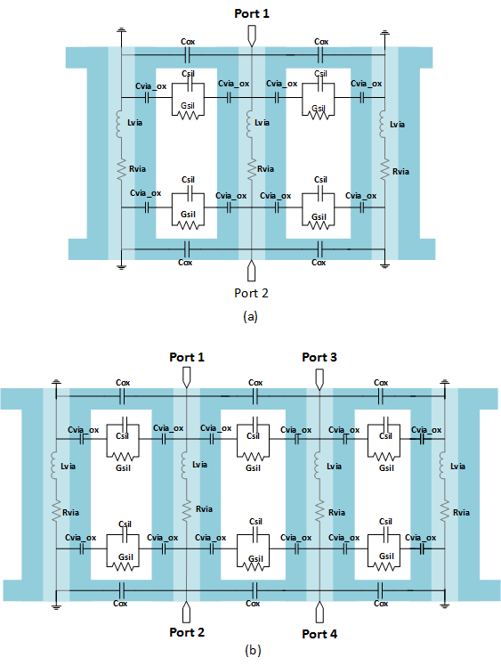 Figure 1: Equivalent Circuit Model of (a) a Standard GSG TSV and (b) a standard GSSG TSV [12]
3. 3D GTL I/O Testing
3.1. Single-Ended Gunning Transceiver Logic (GTL) I/O Design
Single-ended GTL (Gunning Transceiver logic) I/O standard is used in a wide range of applications from ASICs and processors to interface logic devices. A GTL I/O test structure [13] consists of a GTL clock and data receiver, data depths control logic, a serial-to-parallel converter, and GTL I/O drivers as shown in Figure 2. The GTL clock and data can be provided from off-chip using an external test equipment. The data depth control logic controls the depth of the fired data where the control signals come from an external stimulus system. The serial-to-parallel converter loads the serial data from off-chip and fire the parallel data out to the I/O ports. The basic cell consists of a flip-flop and a multiplixer that selects either the serial or parallel data. When the shift register goes to the parallel mode, the register starts firing the parallel data indefinitely with period specified by number of GTL cells. GTL I/O driver is basically an open drain circuit. The circuit has NMOS shunted to ground, and the other end is pulled up to the termination voltage with a 50Ω off-chip resistor.
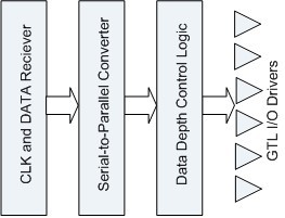 Figure 2: A GTL I/O test structure
3.2. GTL Circuit Architecture in 3D Stacked ICs
A Gunning Transceiver Logic (GTL) I/O test circuit can be utilized to characterize the performance of the 3D TSVs under high speed transient simulation in 3D stacked ICs. The 3D GTL I/O test circuit will fire different data patterns at different frequencies having different data depths across multiple tiers to characterize the impact of TSVs by observing the transient performance through different 3D routes. Figure 3 shows a block diagram of the proposed test structure, where the GTL serial-to-parallel shift registers (SIPOs) are placed in different tiers. A control MUX with Tri-state buffers and control logic can be used to switch between different I/O signals. Figure 4 shows the 3D GTL I/O circuit implementation, where each tier has a 16-bit serial IN-2-bit parallel out GTL test structure. Each I/O driver fires signals out through TSVs from its corresponding tier.
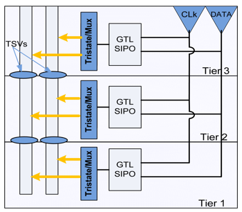 Figure 3: The GTL I/O Test Structure in 3D Stacked IC
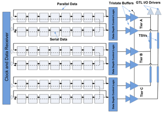 Figure 4: 3D GTL I/O Circuit Implementation
The 3D GTL I/O test structure can be also dedicated to measure the NEXT/FEXT crosstalk between vertical connections by firing high speed signals from different tiers as shown in Figure 5. FEXT and NEXT crosstalk tests can be realized by activating only the I/O signal in tier A and tier C respectively. For example; FEXT crosstalk can be observed by firing high speed signal only at the bottom layer and monitoring the coupling noise at the far-end of the victim line. Similarly, NEXT crosstalk can be observed by firing high speed signal only at the top layer and monitoring the coupling noise at the near-end of the victim line.
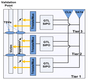 Figure 5: Measuring Crosstalk between TSVs in 3D Stacked ICs
A 2 port GTL I/O test for three tiers system was designed and simulated using the Advanced Design System (ADS) and 0.13 µm UMC CMOS process. Figure 6 shows the simulated results of the GTL test circuit at 1Gb/s data rate.
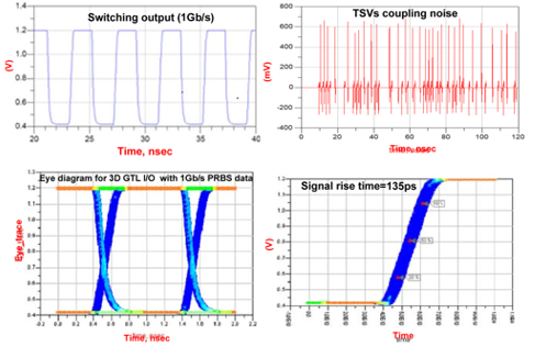 Figure 6: simulated 3D GTL Test Results at 1Gb/s data rate.
3.3. TSV Test Using the GTL I/O Shift Register as Scan Chain
A testing scheme for TSVs in 3D ICs can be realized by using the Gunning Transceiver Logic (GTL) shift register circuit. The GTL serial-to-parallel (SIPO) shift register can be designed where the TSVs are connected serially to form a scan chain structure [14]. In this case, each TSV is connected to a multiplexer and a flip-flop which can be used as scan chain as shown in Figure 7. When the GTL registers are in the data load mode, the registers start loading data serially from the top tier and shifting them down and up between tiers. After loading the data, data starts circulating up and down and vice versa. Circulating data with different patterns can test the reliability of TSVs.
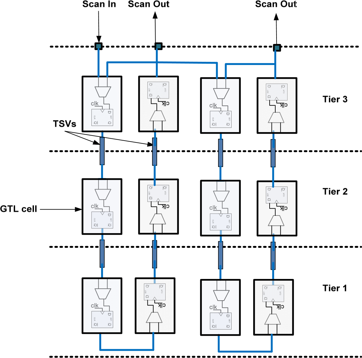 Figure 7: The GTL serial-to-parallel shifts register for 3D TSV test
The GTL scan chain test structure was simulated using ADS and 0.25 µm standard CMOS process. The TSVs connect the GTL cells serially between tiers. The TSVs are tested by injecting test vectors (i.e. data patterns) in one tier (source tier). The test vectors are then propagated to the destination tier (e.g. the top tier), where they are captured and transmitted off-chip. Figure 8 shows a test vector with data stream (“101010..”), which is injected from the source tier and captured at the destination tier (i.e. top tier). In case of faulty TSVs, the captured data has bit errors as shown in Figure 8(b).
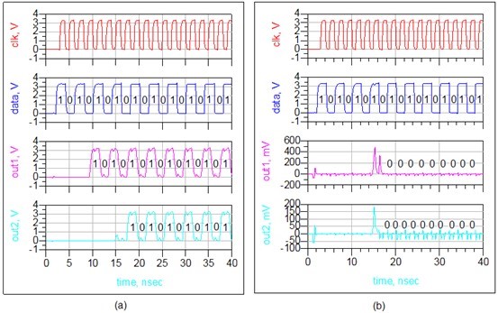 Figure 8: Outputs of the scan chain using the GTL shift register (a) with fault-free TSVs (b) with faulty TSVs.
4. Oscillation Ring-based 3D Testing Schemes
Oscillation ring (OR) test is a useful and efficient method to detect faults in functional circuits and devices [15-16]. An oscillation ring is a closed loop with an odd number of signal inversions. Intuitively, if an oscillation ring fails to oscillate, it implies that there exists stuck-at or open faults in the components of the oscillation ring. The period of the oscillation signal can also be measured to test the delay faults. For example; in a circuit with gate or path delay faults, the oscillation frequency is different from the fault–free circuit. By observing the oscillation signal at the circuit output, one can decide whether the circuit-under-test is faulty or not. To evaluate the impact of a TSV on 3D circuit performance due to the additional delay induced by a TSV, an Oscillation Ring (OR) 3D Built-in Self-Test (BIST) testing schemes, shown in Figure 9, are designed and simulated using the Advanced Design System (ADS) and 0.25 µm standard CMOS process. The target fault models of this testing architecture are TSV stuck-at, open, delay and slope degradation, and TSVs strong crosstalk coupling. If a triggered oscillator fails to oscillate, there exist stuck-at or open faults in the components of the RO. In addition, measuring the TSV delay fault can also be achieved. In this proposed testing scheme, a counter is included at the output of each triggered oscillator to detect TSVs delay faults.
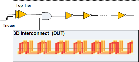 Figure 9: OR Testing Methodology for 3D Stacked ICs
4.1. TSVs Test with Different Configurations
In this testing scheme, a parallel ring oscillators (ROs) testing structure is presented, each RO has different routing TSVs configuration across different stacking tiers as shown in Figure 10. An edge detector circuitry is used to trigger ROs in parallel when the trigger enable signal (OR_TEST) is asserted and a rising edge of the reference clock is detected. This will imply that each one will have a different oscillating frequency and thus a different counting value, which can be scanned out for off-chip testing. Since the frequency of each triggered oscillator is predetermined during the design phase, a delay fault can thus be detected and measured by inspecting the contents of the counters. In this test scheme, let assume that we have m triggered oscillators for different TSV configurations and the oscillation ring test is enabled by the OR_TEST signal. Also let assume that the triggered oscillator unloaded by TSVs is allowed to count only up to n at frequency of f0 and the counter contents of the other triggered oscillators, be n1, n2, …, nm, respectively. An estimation of the ith ring‘s oscillation frequency fi can be approximated by:
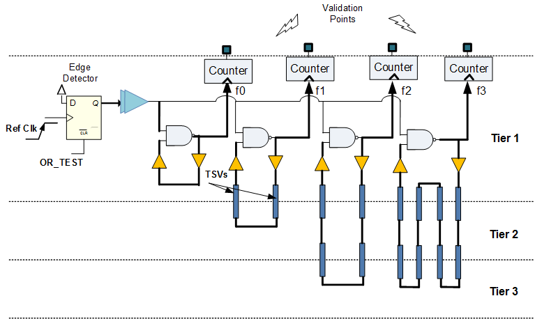 Figure 10: 3D Interconnect Test based on a Parallel triggered ROs Structure
Figure 11 shows simulation results for the triggered oscillators connected with different 3D configurations based on the pi-model which is used to electrically characterize the TSV. Each triggered oscillator has different output frequencies where the triggered oscillator with unloaded TSV has the highest frequency (1.37 GHz) compared to the ones loaded by TSVs. For example; the triggered oscillators loaded by 2 TSVs, 4 TSVs, and 8 TSVs have the following frequencies: 662 MHz, 543 MHz, and 436 MHz respectively. Each output frequency will have a different counter value. Figure 12 shows the counting values ‘b111, ‘b101, ‘b010 for the 2 TSVs, 4 TSVs and 8 TSVs respectively. Obviously, the addition of a TSV is similar to the addition of a short interconnect, thus leading to a degradation of rise time and more induced delay in the ring oscillator and thus slower oscillating frequency.
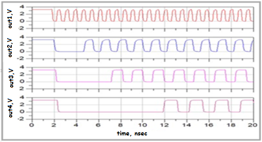 Figure 11: Output frequencies for the triggered oscillators
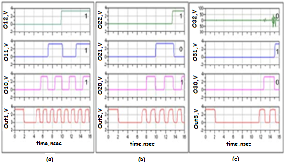 Figure 12: Output Frequencies and Counter Values for Different 3D Configuration (a) TSVs, (b) 4 TSVs, (c) 8 TSVs
4.2. TSVs Rise Time Degradation Test
To characterize the effect of the rise time degradation using the OR test, the capacitance of the thin oxide layer is changed from 10fF to 4pF, which corresponds to 45 ps, and 1.3 ns rise time respectively as shown in Figure 13. This will presents the importance of RC delay caused by the time needed to load TSV oxide capacitance. Figure 14 shows the output frequency and the counter values for triggered oscillators loaded by 2 TSVs for both cases (45 ps, 1.3 ns). The 1.15 Ghz output frequency with counter value of ‘b111 corresponds to the 45ps TSV rise time, and the 833 MHz output frequency with counter value ‘b010 corresponds to the 1.3 ns TSV rise time.
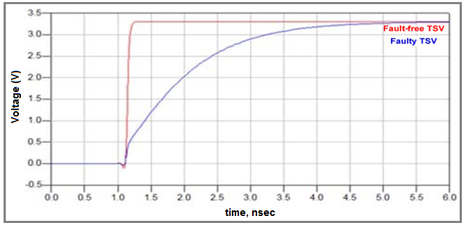 Figure 13: TSV Rise Time (red: 45ps, blue: 1.3ns)
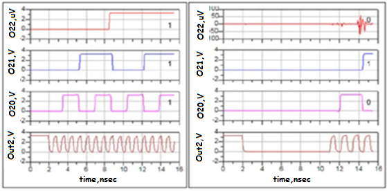 Figure 14: Output Frequencies and Counter Values for (a) 45ps TSV rise time, (b) 1.3ns TSV rise time
4.3. TSVs Crosstalk test
In this test, a consecutive triggered parallel ROs structure running same frequency is used to characterize the crosstalk effect between TSVs. Figure 15 shows four triggered oscillators; two oscillators are crosstalk-coupled and the other two are crosstalk-free. The proposed ROs parallel structure creates a delta phase shift difference between each consecutive triggered oscillators, which is equal to the time difference between the delay buffer chain and the oscillation time period of the triggered oscillators. 3D crosstalk detection can be achieved by observing the frequency of crosstalk-coupled oscillators, which is different from the frequency of the crosstalk-free oscillators.
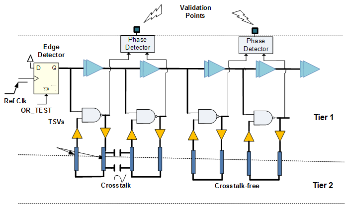 Figure 15: 3D Crosstalk Detection Scheme
Figure 16 shows the output frequency for both crosstalk-coupled (725 MHz) and crosstalk-free oscillators (667MHz).
 Figure 16: Output frequency for (a) Crosstalk-coupled and (b) Crosstalk-free oscillators
Interestingly, the two crosstalk-coupled triggered oscillators have less oscillation time delay (i.e. faster frequency) than the crosstalk-free oscillators, and the phase difference between the two crosstalk-coupled oscillators diminishes due to the coupling effect as shown in Figure 17. Phase detection at the output of the crosstalk-coupled triggered oscillators can be used as an indicator for strong coupling between TSVs. On the other hand, the edges of crosstalk-free oscillators are still separated by a deterministic phase shift dictated by the time difference between the delay buffer chain and the ring oscillation time period.
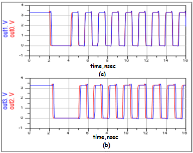 Figure 17: Simulated Results for 3D Interconnect Crosstalk (a) Crosstalk-coupled (b) Crosstalk free
5. Conclusion
In this paper, on-chip testing techniques are presented to test and characterize the signal integrity effects of TSVs after fabrication. Characterizing TSVs using an on-chip 3D testing will provide accurate information since it is closely matches real IC operating conditions, which is very important to evaluate the 3D circuit performance and validate the electrical models of these TSVs. In this paper, 3D testing techniques for TSVs are presented. A Gunning Transceiver logic (GTL) testing structure is utilized to provide a unique way of characterizing crosstalk and Inter-Symbol-Interference (ISI) effects of TSVs. This includes a proposed methodology of characterizing near-end crosstalk (NEXT) and the far-end crosstalk (FEXT) between different 3D routes. A GTL shift register can be also utilized as scan chain test to characterize the reliability of TSVs. Finally, an oscillation ring (OR) 3D testing methodology to detect and identify faulty TSVs and characterize their impact on 3D circuits performance is presented. The proposed OR testing methodology adopt a parallel ROs structure, which is dedicated to detect TSV faults such as stuck-at, open, delay faults and crosstalk coupling between TSVs. The parallel RO structure can be built in different 3D configurations connected through TSVs across different 3D stacking tiers to evaluate and characterize the reliability of TSVs. For open and short faults, the circuit outputs of this test scheme are based on pass/fail criteria. TSVs delay and rise time degradation can be detected based on the counter data for each triggered RO. In addition, the proposed testing structure provides a new way of detecting a strong noise coupling between TSVs. In this test, the outputs of the coupled ring oscillators, which is running at same frequency, will eventually lock in phase due to the coupling noise between TSVs, where a phase detection circuit can be used to indicate a strong TSVs crosstalk noise.
- J. Q. Lu, “3-D Hyperintegration and Packaging Technologies for Micro-Nano Systems,” in Proc. of IEEE, vol. 97(1), 2009, pp. 18-30.
- W.R. Davis et al., “Demystifying 3DICs : the Pros and Cons of Going Vertical”, IEEE Design and Test of Computers, vol. 22, no. 6, pp. 498 – 510, 2005.
- R. Wang, K. Chakrabarty, S. Bhawmik,“At-speed interconnect testing and test-path optimization for 2.5D ICs,” in Proc. IEEE VLSI Test Symp. (VTS), 2014, pp. 1-6.
- R. Weerasekera, M. Grange, et al., “Compact modelling of throughsilicon vias TSV s in three dimensional (3D) integrated circuits,” in IEEE Int’l Conf. on 3D System Integration, 2009, pp.1-8.
- W. Yao, S. Pan, et al., “Modeling and application of multi-port TSV networks in 3-D IC,”IEEE Trans. Comput.-Aided Design Integr. Circuits Syst., vol. 32, no. 4, Apr. 2013., pp. 487-496.
- Z. Xu, A. Beece, et al., “Crosstalk evaluation, suppression and modeling in 3D through-strata-via (TSV) network,” in Proc. IEEE Int. Conf. 3D Syst. Integr., Nov. 2010, pp. 1-8.
- A. Mercha et al., “Comprehensive analysis of the impact of single and arrays of through silicon vias induced stress on high-k/ metal gate CMOS performance,” in Proc. IEEE Int. Electron Devices Meeting (IEDM), San Francisco, CA, USA, 2010, pp. 2.2.1–2.2.4.
- Shadi MS Harb, William Eisenstadt, “Oscillation ring testing methodology of TSVs in 3D stacked ICs,” IEEE Nordic Circuits and Systems Conference (NORCAS), 2016.
- D. M. Jang, C. Ryu, K. Y. Lee, B. H. Cho, J. Kim, T. S. Oh, W. J. Lee, and J. Yu, “Development and evaluation of 3-D SiP with vertically interconnected through silicon vias (TSV),” Proc 2007 Elect. Comp. and Tech. Conf, pp. 847-852, 2007.
- C. Ryu, D. Chung, J. Lee, K. Lee, T. Oh and J. Kim, “High frequency electrical circuit model of chip-to-chip vertical via interconnection for 3-D chip stacking package,” IEEE 14th Topical Meeting on Electrical Performance of Electronic Packaging, pp. 151-154, 2005.
- Z. Xu, A. Beece, K. Rose, T. Zhang, and J. Q. Lu, ”Modeling and evaluation for electrical characteristics of Through Strata Vias (TSVs) in three-dimensional integration,” IEEE 3D System Integration Conference, 2009.
- C. Ryu, J. Lee, H. Lee, K. Lee, T. Oh, and J. Kim, “High frequency electrical model of through wafer via for 3-D stacked chip packaging,” Electronics System integration Technology Conference, vol. 1, pp. 215-220, 2006.
- A. JongShick, and W. R. Eisenstadt, “In-situ characterization of high speed I/O chippackage systems,” PhD thesis, University of Florida, 2007.
- I. Loi, S. Mitra, T. H. Lee, S. Fujita, and L. Benini, “A low-overhead fault tolerance scheme for TSV-based 3D network on chip links,” IEEE/ACM Int. Conf. ComputerAided Design, pp. 598–602, 2008.
- M. Kaneko, and K. Sakaguchi, “Oscillation fault diagnosis for analog circuits based on boundary search with perturbation model,” IEEE ISCAS, pp. 93-96, 1994.
- K. Arabi, and B. Kamiska, “ (OBIST) scheme for functional and structural testing of analog and mixed-signal integrated circuits,” Int’l Test Conf. pp. 786-795, 1997.