Optimizing the front-end power solution for automotive ADAS systems

Adv. Sci. Technol. Eng. Syst. J. 2(3), 1647–1653 (2017);
 DOI: 10.25046/aj0203204
In this paper the front-end power solution for automotive ADAS electronic systems is analyzed. The increased complexity of electronic systems in ADAS automotive brings new challenges for hardware design, especially with regard to improving the efficiency of the switched-mode power supply while maintaining the overall cost reasonably low and keeping the occupied area on the PCB as small as possible. Four topologies of Non-inverting step-up/step-down converter are analyzed. A real-life case is considered and 4 DC-DC converters are designed and simulated to fulfill the requirements. Finally a comparison between the circuits is undertaken. Results are analyzed from the point of view of efficiency, area and price and a decision is reached for the most optimized converter.
1. Introduction
This paper is an extension of work originally presented in 2016 at the 12th IEEE International Symposium on Electronics and Telecommunications (ISETC) [1].
Advanced driver assistance systems (ADAS) are probably the fastest-growing electronic systems in the automotive industry. Every year more and more features are added to the cars to make them safer and to help drivers. A brief list of the kind of feature available today is as follows: pedestrian detection, traffic sign recognition, blind spot monitor, lane departure warning, forward collision warning, driver monitor, adaptive cruise control and emergency braking control, and the list can continue. This extraordinary increase in available ADAS brings to reality something that once was just a dream or a nice theme for Sci-Fi movies: autonomous car. Researches and trials for self-driving cars have a long history of about 100 years. But only in the last 10 years have notable results been achieved. ADAS are basically the foundation of the self-driving vehicle. Today there are already cars on the road with self-driving features with the most advanced publicly available systems being at Level 2 of autonomy (based on SAE Society of Automotive Engineers International’s J3016 document definition [2]). Level 3 cars are expected to be on the road in 2018.
To support all these features for ADAS and autonomous driving, electronic systems in cars are very complex. To be able to detect the environment many sensors of different types must be available and the information collected must be processed extremely fast. Systems for ADAS and autonomous driving utilize today the following: cameras (4-12), ultrasonic sensors (12-20), radar (short and long range) and LiDAR. Each of these sensors has its own specific capability and by combining the information from them the system is more capable of reading the world around the car.
However the next challenge is to process the huge amount of data received from all these sensors. In a sense self-driving cars will be extremely powerful computers on wheels.
Extremely powerful multi-core processors like Renesas R-Car, Nvidia Parker, EyeQ4 from Mobyleye, etc. are available. Electronic control units (ECU) that can handle and process such large amounts of data are usually multi-processor systems with 1-4 processors and 1 – 2 microcontrollers (MCUs). Such ECU contains also all the required digital interfaces and decoding blocks necessary to capture data from external sensors. Power consumption and power dissipation for these ECUs is important and becomes critical in the automotive context. High requirements for robustness and reliability combined with the need for a long life (10 years) usually demands passive cooling (i.e. with no fans) for the vehicle’s electronics. This is not easy to achieve when the ambient temperature can reach 85°C. These are some of the reasons that compel hardware design engineers to focus on reducing the power consumption and power dissipation of its devices. Besides selecting modern ICs (advanced technology) one can reduce the dissipated power by increasing the efficiency of local power supplies.
The following pages cover the topic of selecting and designing the optimised front-end power supply for ADAS electronics and examine several crucial aspects for automotive use:
- Efficiency, with the overall goal of reducing power loss;
- Board occupied area, considering that the PCB is one of the most expensive parts in an ECU;
- Price reduction, which is the goal when the technical and quality aspects are fulfilled.
2. Power supplies in automotive
Most of the cars in the world today use 12-volt automotive electrical systems. Typically a car battery operates with a voltage in the range of 9V to 16V. Therefore, all electronic circuits powered by the battery power line should be able to account for this input-voltage variation. For modern electronics with most ICs powered at 3.3V or below (2.5V, 1.8V, 1.2V, 1.1V and lower) and only a few ICs that still require 5V or higher (CAN, Flexray, LIN transceivers), this input voltage range (9-16V) seems to be perfect. However, if for the battery the normal voltage is 12V (engine off) and 14.4V (engine on), this also can fall to 7V (warm / hot start) or as low as 3.2V (during cold start) or increase to as high as 34V (load dump).
Figure 1 and Figure 2 show typical warm and cold start profiles, while Figure 3 presents the typical load dump [3]
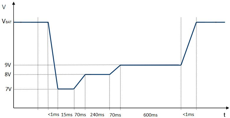 Figure 1. Example of a warm start profile
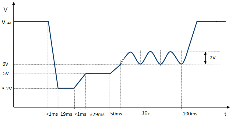 Figure 2. Example of a cold start profile
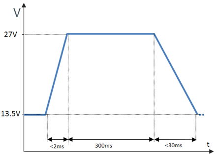 Figure 3. Example of a load dump profile
Voltage levels and timings presented in these figures are typical but they can vary from one car manufacturer to another. They are also dependent on the location of the ECU in the car. Standard profiles for these events are described by ISO 7637-2.
Some electronic systems in the car (engine ECU, safety systems, navigation, infotainment, dashboards, etc) must be live during a cold-crank event and also during a warm start with the requirement to be in Functional Status A: the system must fulfill all functions during and after exposure to the event.
In conclusion many electronic circuits for automotive must be designed to be powered from batteries with a voltage range of 3V – 34V. This wide voltage range is challenging from at least two aspects:
- Minimum input voltage is around 3V and is below some very common voltage rails needed for ICs like 3.3V and 5V. This leads to the need for a way to boost the input voltage to the required levels.
- Maximum input voltage is much higher than the usual rails for the processor’s cores (1V, 0.8V or even lower). It is difficult to directly step down a high voltage like 34V, to a level like 0.8V because the duty cycle is very small. The minimum duty-cycle is limited by the converter’s minimum ON time and its switching frequency. For such a low duty cycle it is highly likely that the step-down converter enters into “pulse-skipping” mode with the risk of increased output voltage ripple and a shift in frequency. Both effects might be unacceptable and result in a high voltage noise that is too high and the risk of failing EMC (electromagnetic) emissions.
To solve both above-mentioned aspects one can use the power supply topology presented in Figure 4. Below can be found a typical block diagram for a power supply system based on an intermediate voltage rail. This is probably the most used power supply topology for complex ECUs in automotive.
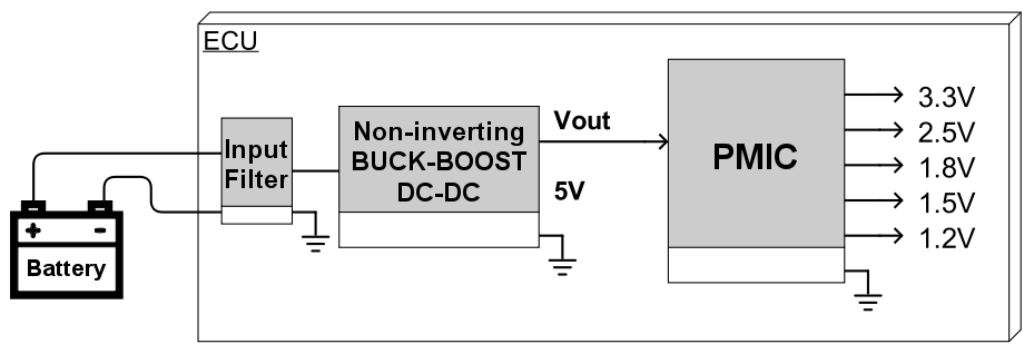 Figure 4. Typical block diagram for an automotive power supply
For this case where the intermediate regulated power rail is VOUT=5V, if the cold start profile goes below 5V, a front-end step-up/step-down DC-DC is required. In Figure 4 this converter is mentioned as being Non-inverting BUCK-BOOST because the input voltage range can be below or above the output voltage (5V) and the output voltage has the same polarity as the input one. 5V as output of the front end power supply is not a magic number, but it is a suitable value for at least 3 reasons:
- A 5V rail is still needed in the automotive electronics for circuits like CAN, and Flexray;
- Most of the available power management ICs (PMIC) have a maximum input voltage of 5.5V;
- A lower value for the output of the front-end supply brings the converter into the zone of very low duty cycles and the associated risks and issues.
3. Non-inverting Step-up/Step-down converter topologies
In the literature, there are few DC-DC converter topologies that can produce the non-inverting step-up/step-down function [4]. Some of them, such as BOOST-BUCK and SEPIC are well-known, whereas others such as 4-switch BUCK-BOOST and ZETA are not so popular. One solution is to use two-stage conversion: one BOOST is followed by one BUCK (BOOST-BUCK). Another approach is the single-stage buck-boost converters such as: 4-switch BUCK-BOOST, SEPIC or ZETA.
3.1. BOOST-BUCK converter
Figure 5 shows the Boost-Buck converter with two implementations: a) asynchronous and b) synchronous. This converter is basically a cascade of two converters, a BOOST formed by L1, Q1, Q3 (or D1) and C1 followed by a BUCK made by Q2, Q4 (or D2), L2 and C2. The purpose of the Boost converter is to provide a minimum intermediate voltage Vmid during cold or warm start battery voltage sags. Vmid is set to provide enough input voltage for the Buck converter. As long as Vin > Vmid the Boost converter is disabled and the Buck converter is powered through L1 and Q3 (or D1). For this case Q3 or D1 are ON and Q1=OFF. During this phase Vmid is not regulated and is: Vmid=Vin-V(L1)-VDS(Q3) for the synchronous converter or Vmin=Vin-V(L1)-VF(D1) for asynchronous one.
When Vin ≤ Vmid the boost converter kicks in and maintains Vmid as a regulated voltage.
- Asynchronous
- Synchronous
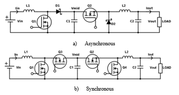 Figure 5. BOOST-BUCK converter
3.2. 4 switch BUCK-BOOST converter
Another topology capable of producing a positive regulated output voltage for Vin below or above Vout is the synchronous 4-switch Buck-Boost – Figure 6 a) and b).
- Asynchronous
- Synchronous
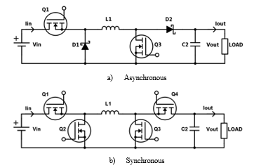 Figure 6. 4-Switch BUCK-BOOST converter
Basically, this is a simplification of one BUCK converter followed by one BOOST converter; both converters share the same inductor L1 [6]. There are 3 modes of operation based on the relationship between Vin and Vout:
- Vin much higher than Vout → Buck mode
Q3 is constant OFF and Q4 (or D2) is constant ON. This is the preferred mode of operation because the efficiency is good. This is basically a buck converter’s efficiency reduced by the Q4 loss in constant conduction (Iout*Rds(on)). However, for the asynchronous version, Q4 is replaced by a diode D2 and there could be important power loss due to the forward voltage of the diode being continuously ON (Iout*VF(D2)). If the output voltage Vout selected is low enough (e.g. 5V), this mode of operation is the mode of operation for most of the time, normal operation, warm start and load dump. So it is important to minimize the power loss produced by the inactive Boost section.
- Vin much lower than Vout → Boost mode
Q1 is constant ON and Q2 (or D1) is constant OFF. If Vout=5V, according to Figure 2, the converter will work in this mode only for about 20ms (lowest section of the cold start profile).
- Vin close to Vout → Buck-boost mode.
In this mode all 4 transistors are controlled by the driving controller to ensure a proper transition from Buck to Boost or vice-versa. The converter will work in this mode only for few hundreds of milliseconds, when the battery is recovering from the cold crank.
3.3. SEPIC converter
The most common single-stage converter with non-inverting buck-boost behaviour is SEPIC. Asynchronous and synchronous versions are shown in Figure 7. This topology uses only two switches (transistor of diode) [7]. The most known SEPIC configuration is the asynchronous one but here the synchronous SEPIC converter is considered as well [8]. The synchronous SEPIC convertor can be implemented with Q3 NFET (N-channel Field Effect Transistor) of PFET (P-channel Field Effect Transistor) depending on the available driving controller. Overall efficiency of the converter is reduced because two inductors are used in operation and due to high currents and voltages for the switch elements.
- Asynchronous
- Synchronous
 Figure 7. SEPIC converter
3.4. ZETA converter
Zeta is a very similar topology to SEPIC; it is named “inverse SEPIC” and has the topology shown in Figure 8. It has two inductors and two active switches [4]. One of the active switches can be a diode (D1) or a FET (Q2). Like SEPIC the two inductors can be coupled or independent.
- Asynchronous
- Synchronous
 Figure 8. ZETA converter
ZETA topology is better for lower output voltage ripple due to continuous output current in L2. This reduces the required output capacitance to maintain a low output voltage ripple. However due to the input discontinuous current (through Q1) ZETA shows higher input voltage ripple. ZETA convertor can be implemented with Q1 NFET of PFET, depending on the available controller.
3.5. Topology comparison
As previously shown, all 4 types of non-inverting step-up/step-down converters considered here have their asynchronous and synchronous variants. To avail of increased efficiency this work considers only the synchronous type of converters here. This one reduces the power loss associated with diodes in conductions and proves to have higher efficiency for higher current load [5].
Some advantages and disadvantages have been already mentioned but a more detailed comparison is undertaken in Table 1. This table contains two sections, one for advantages for each converter and one for disadvantages [9, 10].
Each type of SMPS presented here has its own advantages and disadvantages, so there is no unique answer to the question: ‘what non-inverting step-up/step-down is the best?’ The final decision in selecting one or another topology belongs to the design engineer based on his application’s requirements. The next section contains a comparison for all these 4 types of converter for a real life case, comparisons that helps the designer to decide what the most optimized converter for an application is.
4. Case study and simulations
A real life case for a front-end power supply was selected to show the differences between these 4 converters. Design requirements are listed in Table 2.
To be able to compare the board occupied area and price for all converters it was decided to use real components, available on the market, components that are automotive qualified. For the same reasons it was decided to use controllers from a single supplier – Linear Technology, now part of Analog Devices [12]. All four designs were simulated using the same Spice simulator – Ltspice.
Table 1. Comparison of advantages and disadvantages for 4 non-inverting step-up / step-down converters
| BOOST-BUCK | 4 switch BUCK-BOOST | SEPIC | ZETA |
| Advantages | |||
| Continuous, non-pulsating input and output currents due to input and output inductors (L1 and L2).
This reduces ripple voltage (input and output) and improves the EMI noise, and can simplify the input filter design and size. |
Single inductor design.
Lower price and smaller board occupied area. |
Only two active switching components are required | Only two active switching components are required |
| Easy to design and compensate. Both converters, Buck and Boost are mature circuits and well known, easy to design and easy to compensate for stability | Switch rating = Vin for input section, Vout for output section => Mosfet transistors with lower VDS can be used, so with better (lower) Rds(on) | Low input voltage ripple | Low output voltage ripple |
| Can be designed using two completely separated controllers / converters | High efficiency | Inherent short-circuit protection at output due to DC-block capacitor | Inherent short-circuit protection at output due to DC-block capacitor |
| Disadvantages | |||
| Two inductors are required: price and area. Inductors are expensive and big components. | Input and output are both noisier due to discontinuous currents Iin and Iout | High output ripple (similar to Boost) | High input voltage ripple (similar to Buck) |
| 4 switches are needed – price | 4 switches are needed | Two inductors are required | Two inductors are required |
| Low efficiency – during normal Vbat range converter works in Buck mode but it has a power loss in L1 and Q3 | The controller for the entire converter is more complex and contains two driver sections | Coupling capacitor C1 is needed. In automotive use two series capacitors might be need to protect against MLCC failure (failure mode is short) | Coupling capacitor is needed but the voltage across it is lower (Vout). Series capacitors might not be needed |
| Controller needed is complex (two driver sections or two controllers) | Special consideration for crossing point between Buck-mode and Buck-mode is needed. | Frequency compensation is more difficult to be implemented | Frequency compensation is more difficult to be implemented. Zeta is not well understood. |
Table 2. Design Requirements for the front-end SMPS
| VIN | 4-35V |
| fsw | 400KHz |
| VOUT_ripple | <50mV |
| VOUT | 5V |
| IOUT | 5A |
The switching frequency is set at 400 kHz as a trade-off between several factors: efficiency, area, cost and EMC risks.
It is known that lower switching frequency improves efficiency due to lower switching losses, but also increases the occupied area (expensive) [11]. Big and expensive inductors and big and expensive capacitors are needed to reduce the input and output voltage ripple. So, higher efficiency at low frequency comes with higher cost [12]. On the other hand, these DC-DC converters must comply with very strict requirements in terms of conducted and radiated EMC emissions. It is very important to avoid generating noise in the radio AM band (535 kHz to 1705 kHz) so the switching frequency should be below or above AM band. Switching frequencies above AM band suffer from low efficiency and might force the controller into pulse-skipping mode during load-dump. So, the switching frequency is selected just below AM band.
All four designs use as a starting point the application notes available from the supplier. The target is to design a stable power supply capable of fulfilling the requirements with the minimum of components. However, to have a fair comparison passive components from the same family/series are used and where possible even the same components are used. This approach helps to obtain a fair comparison in terms of occupied area and price. In Table 3 a BOM comparison is shown as a result of the design of these for SMPS.
Next controllers are used in these designs:
- Boost-Buck – LTC7812
- 4-switch Buck-Boost – LTC3789
- SEPIC – LT8710. Un-coupled inductors are used.
- ZETA – LT3840 Un-coupled inductors are used.
Table 3. BOM comparison
| BOOST-BUCK | 4-switch BUCK-BOOST | SEPIC | ZETA | |
| Controller | Dual:
Boost + Buck |
4 Switch Buck-Boost | BOOST | BUCK |
| L1 | 2.2uH / 14A | 2.2uH / 14A | 2.2uH /14A | 2.2uH /14A |
| L2 | 3.3uH / 8A | – | 3.3uH / 8A | 3.3uH / 8A |
| Q1 | NFET – 40V, 49A, 9.3mΩ | NFET – 40V, 49A, 9.3mΩ | ||
| Q2 | – | NFET – 40V 49A, 9.3mΩ | ||
| Q3 | PFET, 60V 64A, 14mΩ | – | ||
| Q4 | – | – | ||
| CIN – cer. | 1x2x 10uF
50V |
1x2x 10uF
50V |
1x2x 10uF
50V |
1x2x 10uF
50V |
| CIN – Bulk | 150uF / 35V | 150uF / 35V | 47uF / 35V | 150uF / 35V |
| CMid – cer. | 3x 2x 10uF
50V |
– | – | – |
| CMin – Bulk | 270uF / 35V | – | – | – |
| COUT – cer. | 2x 22uF / 10V | 3x 22uF / 10V | 4x 22uF /10V | 1x 22uF /10V |
| COUT –Bulk | 220uF / 6.3V | 220uF / 6.3V | 220uF / 6.3V | 220uF / 6.3V |
| Coupling Cap- Cer.
(Include RC damping) |
– | – | 2x 2x 33uF/
35V |
4x 22uF /
10V |
| Output Ferrite Bead | – | Z=60Ω @ 100MHz | Z=60Ω @ 100MHz | – |
4.1. Simulation results
Due to lack of space only the schematics for 4-switch Buck-Boost converter (Figure 9) and ZETA converter (Figure 10) are provided here.
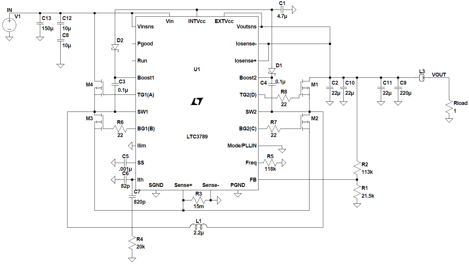 Figure 9. 4-switch Buck-Boost converter schematic
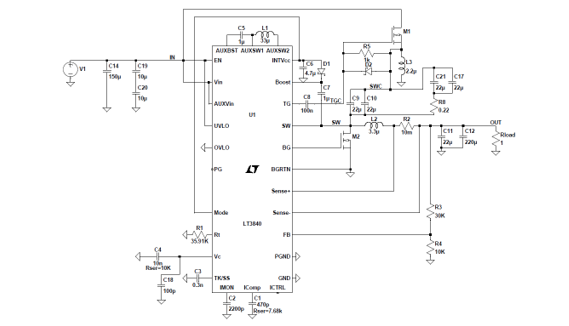 Figure 10. ZETA converter schematic
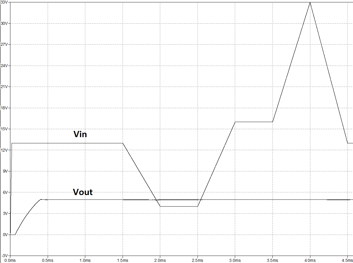 Figure 11. Simulations results for 4-switch Buck-Boost
Figure 11 shows the transient simulation result intended to verify the behavior of the converter when the input voltage Vin varies from 0V to 33V. The response to Cold-crank and Load-Dump events is verified in the same simulation. To speed up the simulation, all the timings from these two profiles are compressed and reduced. However, the converter reacts very well to these faster transitions too.
All simulation results for all 4 considered converters are virtually identical with those shown in Figure 11.
Based on the simulation performed and their results it can be concluded that all 4 designed converters are suitable to be used for the case being considered. All converters can handle the automotive cold-crank, warm-start and load-dump events and provide a regulated output voltage.
4.2. Comparison for efficiency, are and cost
Because all 4 converters are suitable to be used as a front-end power supply for ADAS ECUs (from electrical point of view), one can optimize the power solution for automotive applications by using several criteria:
– Efficiency comparison is shown in Figure 12. Ideally, one would like to select the converter that has the best efficiency over the entire input voltage range for a given output current and system requirements; however, the converter stays a brief time in cold-crank so the efficiency in this phase might be not so important for some applications. The left side of Figure 12 shows the efficiency comparison during cold-crank profile for a weak battery while the right side shows the efficiency for each converter when the battery is healthy.
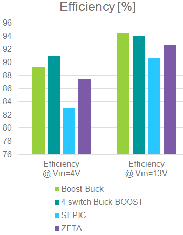 Figure 12. Efficiency comparison
– Occupied area, with and without controller – Figure 13. The entire PCB occupied area by a converter is important and it is shown in the left section of Figure 13. Controller size / package might vary from one supplier to another while the external components remain almost the same so a comparison of the space requirement without the controller is presented in the right side of Figure 13. For comparison of the occupied area the sum of areas of all components was considered plus an additional 0.5mm keep-out area on each side for each component;
– Price with and without controller – Figure 14. Prices used in the comparison are obtained from the supplier website (Linear Tech) for SMPS controller and all the other parts are from component distributor Mouser. Prices are expressed in € and are for 1k pieces.
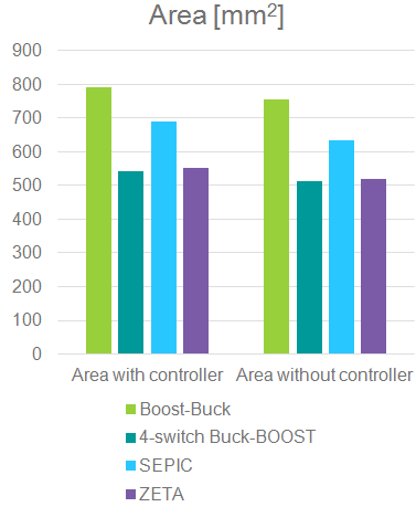 Figure 13. Occupied area comparison
 Figure 14. Price comparison
A summary of these comparisons is available in Table 4.
Table 4. Summary of comparisons
5. Conclusions
Four synchronous converters suitable to perform the non-inverting step-up/step-down function for powering an ADAS electronic system are considered in this work. A short theoretical analysis is presented and a list of advantages and disadvantages of all topologies is undertaken and summarized, from the perspective of automotive applications. One must know all the advantages and disadvantages of all suitable DC-DC converters before being able to obtain an optimized solution. A method of optimization for automotive ADAS front-end power supply is to consider the efficiency, board occupied area and cost along with the quality parameters of an SMPS (not studied in this work) (as input and output voltage ripple, loop response, stability and transient response).
A real life case was considered and according to the simulation results obtained and the comparisons made for efficiency, occupied area and cost, it can be concluded that the 4-switch Buck-Boost converter is the optimal one for the real-life case which was considered. This converter meets all the requirements specified in Table 2 and has the smallest occupied area (calculated with or without controller), has a low price and exhibits high efficiency. The SEPIC converter (with un-coupled inductors) proves to be the worst solution: lowest efficiency, highest cost (due to high voltage coupling capacitors) and almost the biggest PCB occupied area. An interesting solution is ZETA that is very competitive in terms of price and space. Also ZETA shows decent efficiency. However precautions must be taken to properly compensate it in frequency.
Future work is planned to analyze the suitability and performance of new/improved converter topology as multi-phase converters (buck-boost, SEPIC) and multi-switch SEPIC/ZETA [13].
Conflict of Interest
The author declares no conflict of interest.
- B. Dragoi, “On selecting a front-end DC-DC converter for automotive applications”, Electronics and Telecommunications (ISETC), 2016 12th IEEE International Symposium on, 27-28 Oct. 2016
- Taxonomy and Definitions for Terms Related to Driving Automation Systems for On-Road Motor Vehicles, SAE international, http://standards.sae.org/j3016_201609/
- International Standard, “Road vehicles — Electrical disturbances from conduction and coupling. Part 2”, ISO 7637-2, 2004.
- M. Wens, M. Steyaert, “Design and Implementation of Fully-Integrated Inductive DC-DC Converters in Standard CMOS”, ISBN 978-94-007-1435-9, pp.90-99, 2011.
- R. Nowakowski, N. Tang, “Efficiency of synchronous versus nonsynchronous buck converters”, Texas Instrument, Analog Applications Journal, Fouth Quarter, 2009, pp.15-18.
- R.W. Erickson, D. Maksimovic, “Fundamentals of Power Electronics”, Second Edition, Kluwer Academic Publisher, eBook ISBN: 0-306-48048-4, 2004, pp.134-137.
- D. Zhang, “Designing A SEPIC Converter”, Texas Instruments, AN-1484, SNVA168D, April 2008.
- Shashikumari J. and Ramya N, “Design of Synchronous SEPIC and Synchronous Zeta Converter for Stand-Alone Photovoltaic System” IJRSI, vol. III, Issue V, May 2016, pp. 529-551, ISSN 2321 – 2705
- J. Betten. “Synchronous Zeta Converter Outperforms The SEPIC”, How2Power Today, Issue May 2014
- V. Choudhary, “Selecting the right buck-boost converter for wide-VIN rails”, Electronic Products and Technology, www.ept.ca, 18.06.2016.
- A.I. Pressman, K. Billings, T. Morey, “Swittching Power supply Design”, Third Edition, McGraw Hill, ISBN 978-0-07-148272-1, 2009, pp. 20-21
- R. Nowakowski, B. King , “Choosing the optimum switching frequency of your DC/DC converter” , 25.10.2006, http://www.eetimes.com/document.asp?doc_id=1272335
- M-S. Song, Y-D Son, K-H Lee, “Non-isolated Bidirectional Soft-switching SEPIC/ZETA Converter with Reduced Ripple Currents”, Journal of Power Electronics, Vol. 14, No. 4, pp. 649-660, July 2014, ISSN(Print): 1598-2092 / ISSN(Online): 2093-4718
No related articles were found.