Impact of Line Resistance Combined with Device Variability on Resistive RAM Memories

Adv. Sci. Technol. Eng. Syst. J. 3(1), 11–17 (2018);
 DOI: 10.25046/aj030102
In this paper, the performance and reliability of oxide-based Resistive RAM (ReRAM) memory is investigated in a 28nm FDSOI technology versus interconnects resistivity combined with device variability. Indeed, common problems with ReRAM are related to high variability in operating conditions and low yield. At a cell level ReRAMs suffer from variability. At an array level, ReRAMs suffer from different voltage drops seen across the cells due to line resistances. Although research has taken steps to resolve these issues, variability combined with resistive paths remain an important characteristic for ReRAMs. In this context, a deeper understanding of the impact of these characteristics on ReRAM performances is needed to propose variability tolerant designs to ensure the robustness of the technology. The presented study addresses the memory cell, the memory word up to the memory matrix.
1. Introduction
Because data storage and processing solutions are so central to modern technology, many research works are dedicated to pursue new types of computer memory. One of the major goal is to develop a universal memory (i.e. a storage medium that would combine the high speed of RAM with the non volatility of a Flash drive). Additionally, embedded memory is a fundamental component of any electronic system including high-performance System-on-Chip (SoC) and Internet of Things (IoT) devices. In this context, the presented work proposes a reliability analysis of the Resistive RAM memory which considered as a potential universal memory candidate. This study is an extension of work originally presented in [1], with an extension to a whole memory matrix. Moreover, a multilevel storage capability of ReRAM cells is demonstrated at a matrix level.
According to ITRS [2], embedded Non Volatile Memories (NVMs) are occupying a major part of the area of a typical (SoC). Although Flash memory is widely used today, it needs high voltage for Write and Erase operations and has reliability issues that are hard to handle, increasing the cost of circuit design and process integration. Thus, the industry is trying to find a good alternative NVM that can replace Flash memories. Possible candidates include Magnetic RAM (MRAM), ReRAM, Phase Change Memory (PCM), Ferroelectric RAM (FeRAM), etc. Compared to MRAM and PCM technologies, ReRAM technology is still in an emerging phase [3][4]. However, a considerable technological effort is currently driven worldwide to push this technology to prototype level. ReRAM advantages comprise non volatile data storage at low power and latency and high memory density while maintaining device performance and reliability [5]. Moreover, the 3D-staking technology developed for Flash memories can be transferred to ReRAM and the multilevel cell operation scheme of Flash memories can also be achieved in ReRAMs [6].
However, the continuous push for scalability to obtain high-density chips makes the ReRAM technology extremely sensitive to variability, physical defects and environmental influences that may severely compromise its correct behavior [7]. At sub 32nm node, size reduction increases the resistivity of interconnects, inducing a voltage drop along the memory matrix lines, which can cause reliability issues. Indeed, as ReRAM data is stored as two resistance states of the resistive switching device, these memories are sensitive to resistive paths [8]. On top of that, common problems with ReRAMs are related to high variability in operating conditions [9].
In memory devices relying on resistance change such as ReRAMs, complex physical mechanisms are responsible for reversible switching of the electrical conductivity between high and low resistance states. This resistivity change is generally attributed to the formation/dissolution of conductive paths between metallic electrodes [10]. A typical ReRAM device consists of two metallic electrodes that sandwich a thin dielectric layer serving as permanent storage medium making its leakage current close to zero. Oxide-based Resistive Random Access Memory (so-called OxRAM) use transition metal oxides as a dielectric layer. In this study, an HfO2 Oxide-based ReRAM stack is considered [11].
OxRAM cell operation is depicted in Figure 1. After an initial electroforming process, the memory element may be reversibly switched between two distinct resistance states. Electroforming stage corresponds to a voltage-induced resistance switching from an initial very high resistance state (virgin state) to a conductive state. After FORMING, resistive switching corresponds to an abrupt change between a High Resistance State (HRS or OFF state) and a Low Resistance State (LRS or ON state). This resistance change is achieved by applying specific voltage (i.e. VSET and VRES) to SET and RESET the memory cell.
It is important to note that the FORMING stage is the first and most critical step as it determines the switching characteristics during the future operation of the memory cell. Thus, the Forming Resistance State (RFRS) which characterizes the filament creation is a key parameter in terms of reliability. Besides, the forming step requires high voltage levels (more important than VSET and VRES).
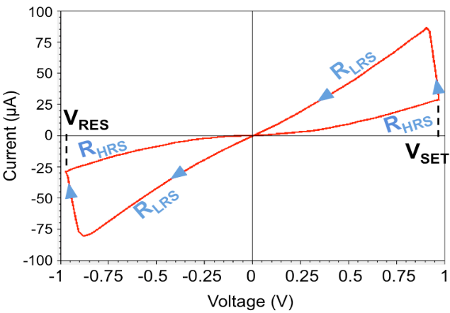 Fig.1: Typical I-V characteristic of a bipolar OxRAM cell
In this paper, the reliability of a ReRAM memory array is investigated versus interconnects and device variability. Section II presents the OxRAM model used for simulations. Section III address a 32-bit memory word. In section III, the study is extended to the memory matrix and the multilevel storage capability of ReRAM cells is demonstrated. Section IV concludes the paper. For each section simulation results based on a 28nm Fully-Depleted Silicon-On-Insulator (FDSOI) are proposed.
2. ReRAM elementary cell model
The proposed OxRAM modeling approach relies on electric field-induced creation/destruction of oxygen vacancies within the switching layer. The model enables continuously accounting for both SET and RESET operations into a single master equation in which the resistance is controlled by the radius of the conduction pathways (rCF) [12]:
![]() Where βRedOx is the nominal oxide reduction rate, Ea is the activation energy, αred and αox are the transfer coefficients (ranging between 0 and 1 and representing the pathways creation/destruction dynamic), kb is the Boltzmann constant, rCFmax is the maximal size of the conductive filament radius, T is the temperature and Vcell the voltage across the cell.
Where βRedOx is the nominal oxide reduction rate, Ea is the activation energy, αred and αox are the transfer coefficients (ranging between 0 and 1 and representing the pathways creation/destruction dynamic), kb is the Boltzmann constant, rCFmax is the maximal size of the conductive filament radius, T is the temperature and Vcell the voltage across the cell.
Moreover, the model makes assumptions of a uniform radius of the conduction pathways, a uniform electric field in the cell and temperature triggered acceleration of the oxide reduction reactions (“redox”). Finally, the total current in the OxRAM includes two components, i.e. one is related to the conductive species (ICF) and the other to the conduction through the oxide (IOX).
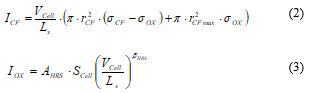 where Lx is the oxide thickness, SCell is the total area of the device, σOx the oxidation rate and σCF the reduction rate. To take into account IOX trap assisted current (Poole-Frenkel, Schottky emission, Space Charge Limited Current (SCLC)), a power law between the cell current and the applied bias is considered with two parameters AHRS and βHRS. Finally, the total current flowing through the cell is:
![]() ICF is the main contributor to LRS current (ILRS) and IOX is the main contributor to HRS current (IHRS).
ICF is the main contributor to LRS current (ILRS) and IOX is the main contributor to HRS current (IHRS).
The memory cell compact model is calibrated on silicon. The model was confronted to quasi-static and dynamic experimental data before its implementation in electrical circuit simulators. As presented in Figure 2a (current voltage characteristic in logarithmic scale), after calibration, the model satisfactorily matches quasi-static and dynamic experimental data measured on actual HfO2-based memory elements (TiN/Ti/HfOx/TiN stack). In Figure 2b, the evolution of SET voltages (Vapp) as a function of the programming ramp speed is presented. The model implementation focused on this dependence which is crucial for the model to be confidently implemented in circuit simulators.
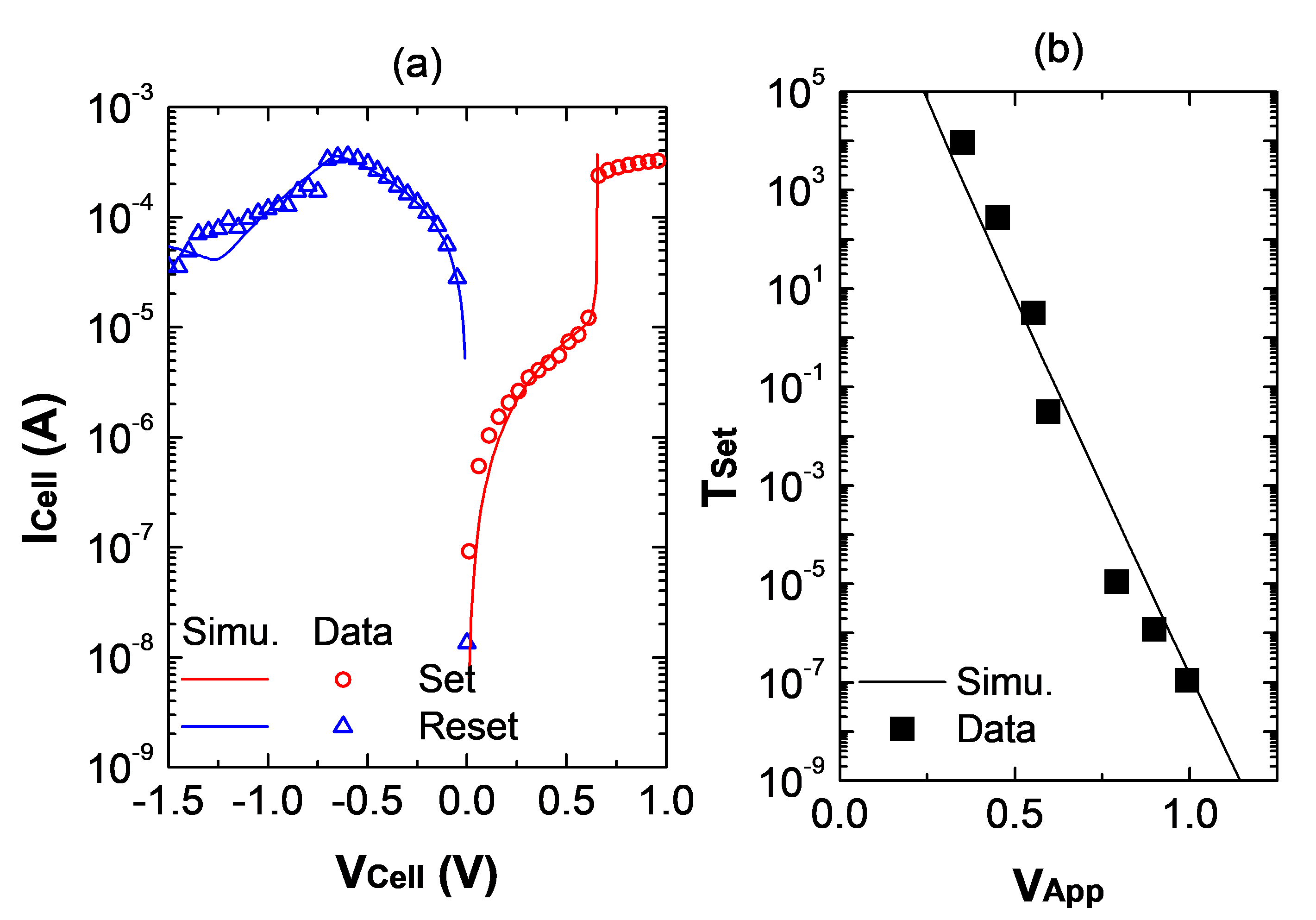 Fig.2: (a) I-V characteristic measured on HfO2-based devices and corresponding simulation using a bipolar OxRAM physical model. (b) SET voltage as a function of the programming ramp
Due to the stochastic nature of the switching process in OxRAMs, leading to large variability, the OxRAM model features a variability dependency. The variation is chosen to fit experimental data as presented in Figure 3. The model behaviour (lines) is consistent with experimental data (symbols). The cell variability modelling is based on OxRAM card model parameters variation. Variability is introduced through specific model parameters (i.e. βRedOx and βHRS parameters presented respectively in Equation 1 and Equation 3). Moreover, at sub 32nm node, MOSFET mismatch in the transistor subsystem (digital and analog blocks) increases inherent variability of OxRAM circuits, increasing the overall variability.
 Fig.3: Measured and corresponding simulated I-V characteristic obtained from TiN/Ti/HfO2/TiN devices showing strong variation on RLHS and RHRS
3. ReRAM memory word
3.1. Memory word architecture
A 1T1R ReRAM cell (one MOS Transistor in series with one Resistor) placed in a 32-bit word is considered and presented in Figure 4. The word selection is achieved through the Word Line (WL) before any operation. Word programming is performed in 2 steps, considering that the FORMING operation occurs only once in the product lifetime. Once the word is selected, all cells are RESET in parallel (logical “0”) through the Reset Word Line (WLR), then memory cells are all SET (logical “1”) through the Bit Line (BL). The WLR line drives the whole word RESET current, making it sensitive to line resistivity.
Indeed, during a memory word program operation, a voltage drop occurs along the WLR line, which can be critical in terms of programming efficiency. To monitor the programming efficiency, High Resistance State (RHRS) and Low Resistance State (RLRS) resistances are extracted after RESET and SET operations respectively.
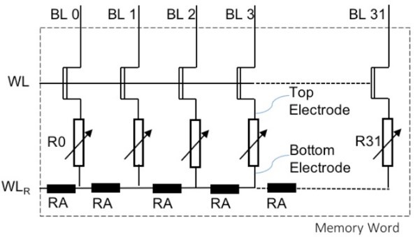 Fig.4: 32-bit ReRAM memory word
The memory word is simulated using the OxRAM model presented in section 2. The model is calibrated on silicon for a 28nm FDSOI technology. With respect to the programming conditions, typical values for LRS and HRS are RLRS=10kΩ and RHRS=130kΩ for the considered technology. The WLR line resistance per cell (including vias) is called RA (see Figure 4) and is evaluated to 1.6Ω [8].
3.2. Simulation results
Impact of line resistances on RHRS and RLRS is presented in Figure 5. The voltage drop induced by line resistances results in a weak FORMING (i.e. high resistive path between ReRAM electrodes). SET and RESET programming levels are thus impacted resulting in a higher RHRS (+5%) and RLRS (+30%) values for cells located at the end of the memory word.
Impact of line resistances combined with variability is presented in Figure 6. After 300 Monte Carlo runs, RHRS and RLRS distributions are extracted for 1 cell over 4 and displayed in box-plot forms. Figure 6a shows that LRS distribution spread increases along the word line. Besides, anomalous LRS residual cell populations (far from their typical LRS values, represented by dashed lines) are visible from cell 7. This effect is related to cells not properly formed due to line resistances. In Figure6b, HRS distributions are presented. One can notice the HRS mean distribution shift to higher values with the word length.
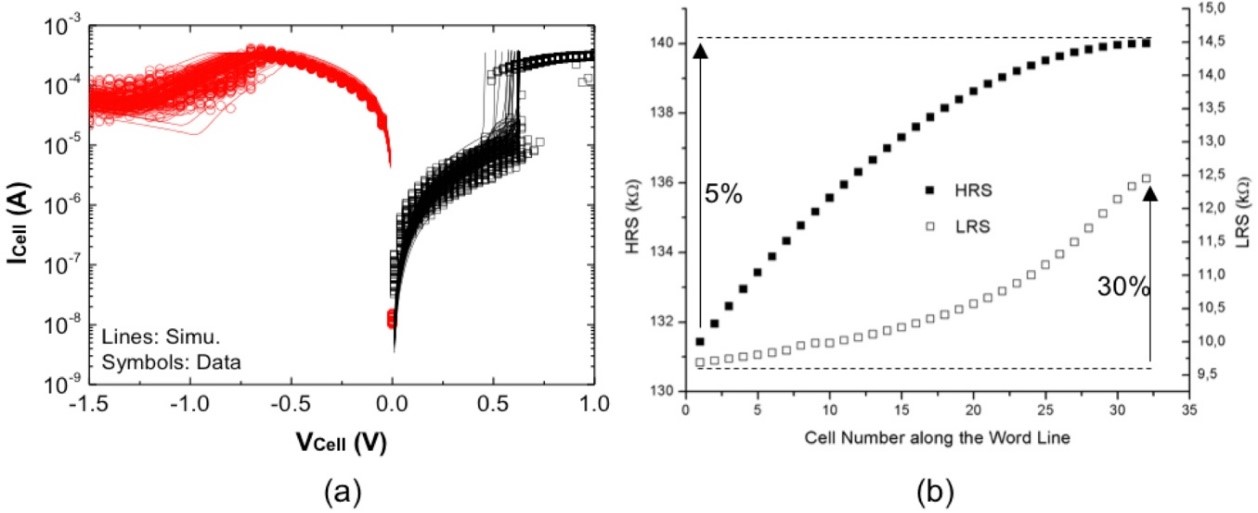 Fig.5: Resistances (HRS & LRS) along the WL
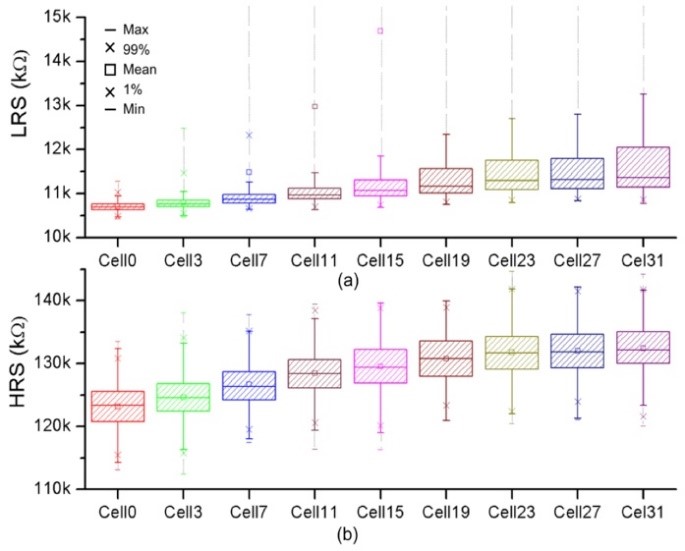 Fig.6: (a) LRS and (b) HRS distributions along the WL
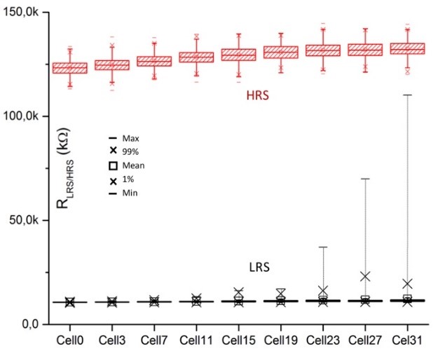 Fig.7: LRS and HRS distributions overlaps along the WL
For comparison purposes, Figure 7 presents the full range variation (from min to max) of each box-plot (HRS and LRS states). Along the WL, HRS/LRS distributions are getting closer and closer due to marginal LRS cells, affecting the memory reliability (i.e. HRS distribution generally larger than LRS distribution is much more degraded by resistive paths).
4. ReRAM memory array
4.1. Memory array architecture
Figure 8 presents the elementary array used for simulation which is constituted by a 3×3 1T1R cell matrix, a row decoder, a column decoder and a sense amplifier for the read operation. The memory cell is modeled by the OxRAM cell model presented in section 2.
The variability analysis is conducted through Monte Carlo simulations. Each Monte Carlo simulation targets specific elements of the circuit: the resistive element, the select transistor, the decoding blocs and the sense amplifier. As a result, RON and ROFF distribution spreads are extracted. Thus, the contribution of each element in terms of memory performance degradation is demonstrated. A 28-nm Fully Depleted Silicon-On-Insulator (FDSOI) technology is considered for simulations [13].
Memory array cells are first placed in a virgin state. Then, the memory array programming is done in 2 cycles. First, all memory cells are set (logical “1”), then the memory array is reset (logical “0”). RON value is extracted after the SET operation and ROFF after the RESET operation for each Monte Carlo run.
Variability introduced in the resistive element is chosen to feet experimental date whereas variability of the transistor subsystem is given by the considered technology.
4.2. Simulation results
In this study, 4 different configurations are considered: the “ALL” configuration considers variability in the memory cell (resistive element and select transistor) and the peripheral circuits. In the “CELL” configuration, variability affects only the resistive element. In the “SELECT” configuration, variability affects only the OxRAM select transistor. In the “NO CELL” configuration, variability affects only the peripheral circuits (transistor subsystem, including the select transistor). In this study, the impact of the select transistor variability is subject to special attention. Indeed, the select transistor compliance allows the control of the maximum available current during the set transition, impacting directly the ON/OFF resistance. Table 1 summarizes the 4 configurations to simulate.
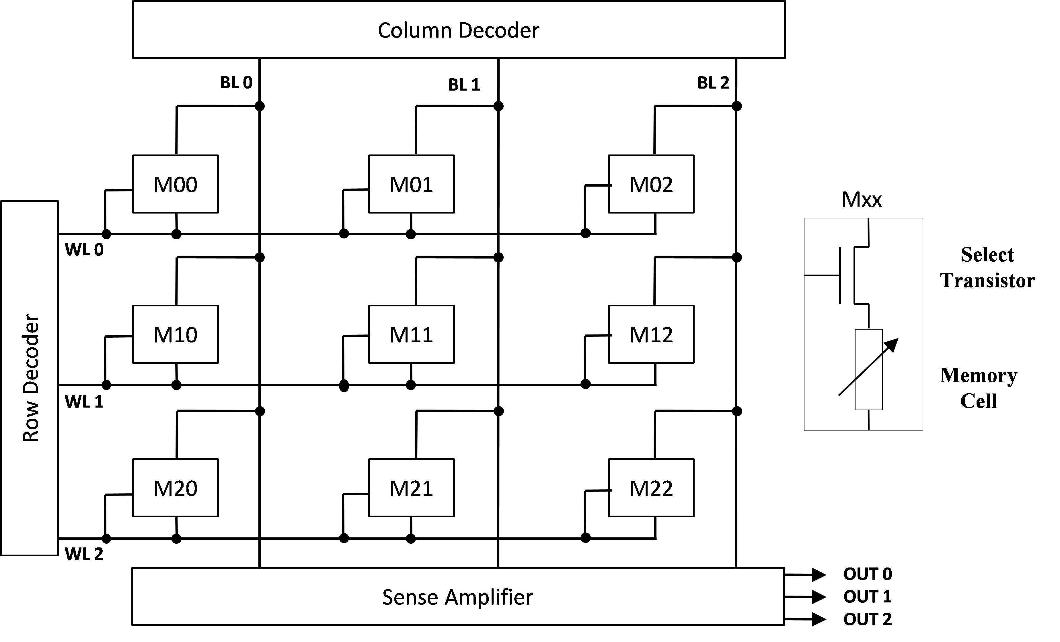 Fig.8: 3×3 OxRAM elementary memory array
Table 1: Simulated Configurations
| Configuration | RUNS | Elements under variability |
| « ALL » | 400 | All circuit elements |
| « CELL » | 400 | Resistive element |
| « SELECT » | 400 | Select transistor |
| « NO CELL » | 400 | All elements excluding the resistive element |
Figure 9 presents the impact of variability of the whole circuit elements (resistive element and transistor subsystem: “ALL” configuration) on RON and ROFF distributions. Note that ROFF distribution is much larger than RON distribution. In order to discriminate the contribution of each element of the circuit on ON/OFF resistances, a set of Monte Carlo simulations are also performed with “CELL”, “SELECT” and “NO CELL” configurations.
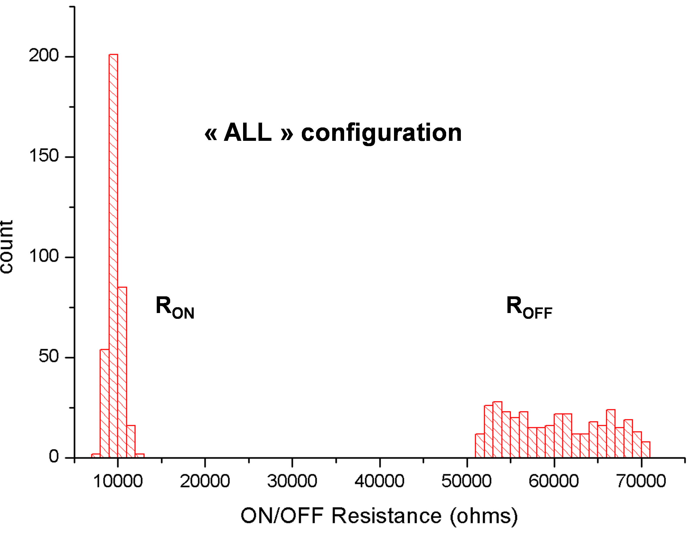 Fig.9: ON/OFF resistance distributions for the “ALL” configuration after 400 Monte Carlo simulations.
Figure 10 presents the impact of variability on ROFF distributions (after RESET) for the 4 configurations. By comparing configuration “ALL” with configuration “CELL”, it appears clearly that the impact of cell variability is more important than the impact of the transistor subsystem variability. The third and fourth configurations (“NO CELL” and “SELECT”) shows that impact of transistors variability on ROFF is negligible. Besides, the contribution of the select transistor variability is dominant in the peripheral circuit elements. Table 2 proposes a synthesis of results obtained in Figure 10 (mean values, standard deviation and standard deviation reported to the maximum standard deviation value).
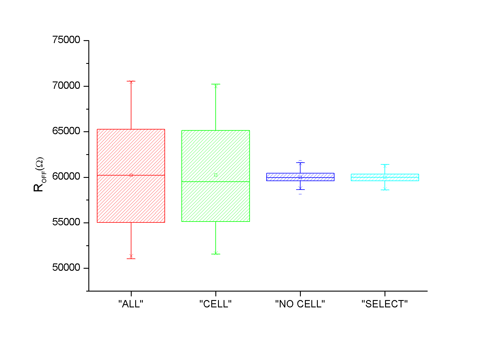 Fig.10: ROFF distributions after 400 Monte Carlo simulations.
Table 2: Roff Distribution parameters
| Configuration | Mean (Ω) | σ (Ω) | σ (%) |
| « ALL » | 60200 | 5598 | 100 |
| « CELL » | 60240 | 5617 | 99 |
| « NO CELL » | 60004 | 598 | 9.6 |
| « SELECT » | 59990 | 536 | 10.6 |
Figure 11 presents the impact of variability on RON distributions (after SET) for the 4 configurations.
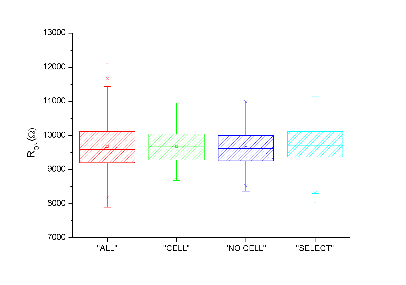 Fig.11: RON distributions after 400 Monte Carlo simulations.
Table 3: Ron Distribution Parameters
| Configuration | Mean (Ω) | σ (Ω) | σ (%) |
| « ALL » | 9674 | 724 | 100 |
| « CELL » | 9679 | 513 | 70.8 |
| « NO CELL » | 9642 | 550 | 78.7 |
| « SELECT » | 9713 | 570 | 75.9 |
Compared to Figure 10, it appears clearly that the cell variability impact is less pronounced for low resistive states (LRS), which is a common feature of all OxRAM technologies [14-15]. Moreover, the contribution of transistors variability is comparable to the contribution of the memory cell variability (see “CELL” and “NO CELL” configurations in Figure 11). Here again, simulation results show that the impact of the select transistor is not negligible. Table 3 proposes a synthesis of results obtained in Figure 11.
Figure12 shows a comparison between RON and ROFF distributions. Based on the considered technology, it is shown that resistance variability in RESET state is much more important than variability in the SET state. This variability is mainly due to the memory cell. In addition, the impact of the select transistor is non-negligible. This effect is visible in the SET state where the impact of the memory cell variability is much less important, making the select transistor variability critical.
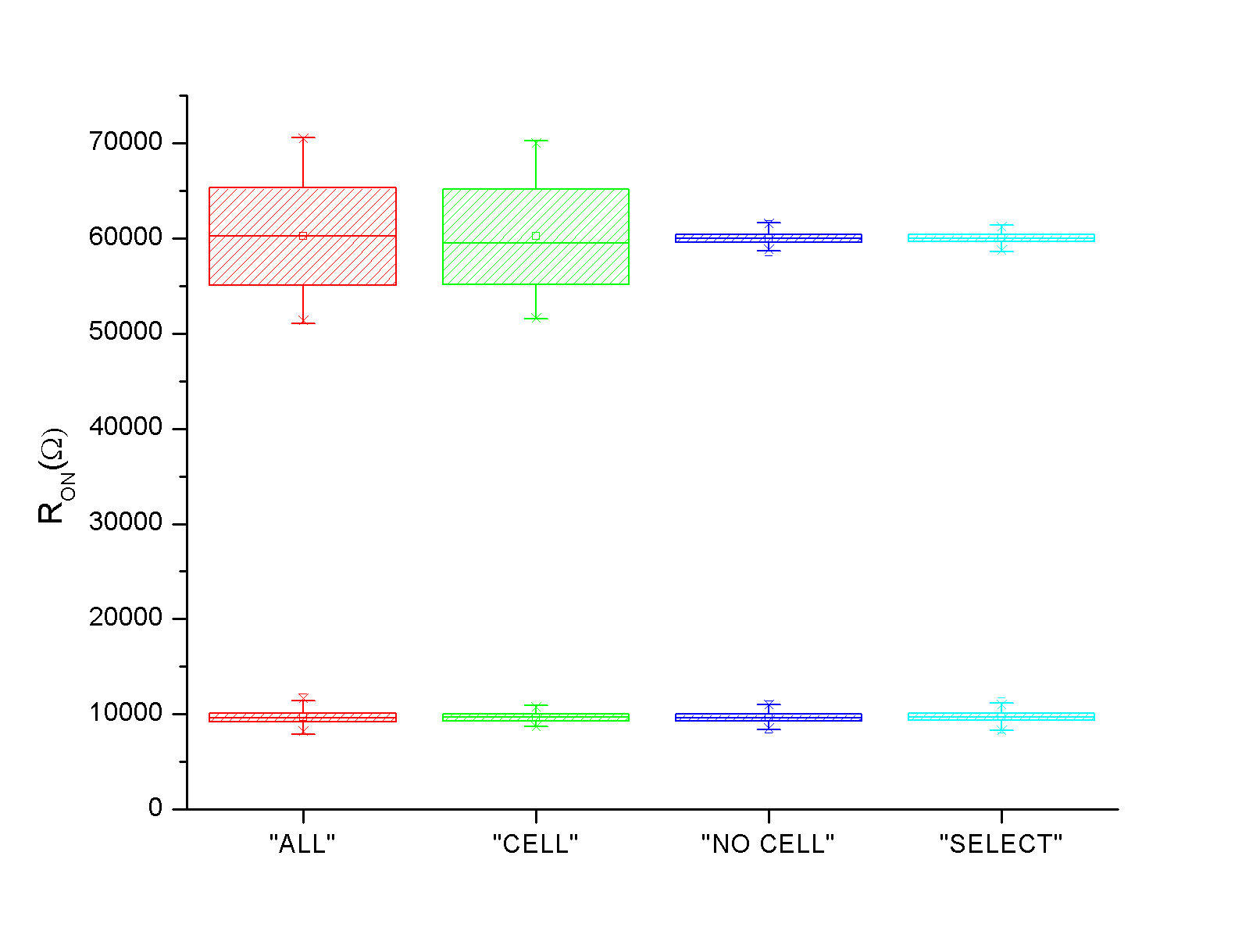 Fig.12: RON/ROFF distributions after 400 Monte Carlo simulations.
4.3. Multi level approach
When a voltage is applied across a ReRAM cell, depending upon the voltage polarity, one or more Conductive Filaments (CFs) made out of oxygen vacancies are either formed or ruptured. Once the CFs are formed inside the metal oxide to bridge the top and bottom electrodes, current can flow through the CFs, and the cell is in a low resistance state. The larger the size of the CFs, the lower the resistance. Conversely, the rupture of the CFs disconnects the top electrode from the bottom electrode, resulting in a high resistance state (HRS) of the cell [16].
According to Equation 1, CF size is directly linked to the voltage across the cell, thus, multilevel LRS can be achieved in the 1T1R RRAM by modulating the SET voltage. In this study, the amplitude of the RESET voltage remains unchanged during the
cell programming operation. As HRS variation is generally larger than LRS variation, multilevel HRS is not considered. The HRS state is associated with an initial value, restored before each SET operation. Finally, to obtain intermediate SET states, programming is done in 2 steps: a RESET operation is first performed to switch the memory cell in its HRS initial state, then a SET operation sets the desired LRS level.
At a circuit level, different implementations of Multi-Level Cell (MLC) operation can be adopted. Multilevel operation can be achieved:
- By applying an increasing number of identical voltage pulses through the SET decoder. In this case, LRS level is function of the number of pulses [17].
- By modulating the gate voltage (WL) of the memory cell Select Transistor to control the SET current [18].
- By modulating directly the SET voltage generated from the SET decoder. In this case, LRS levels are achieved with different SET voltage values.
The first approach requires a pulse generator circuitry while the two others require different voltage levels generated from a specific circuitry. In this study, the third approach is considered as it is the most effective MLC approach for the considered technology. Four different LRS levels are generated by changing the amplitude of the SET voltage. Table 4 presents the different SET and RESET voltages values with the corresponding resistance nominal values.
Table 4: Programming Voltages and corresponding Resistance Values
| SET | RESET | ||||
| Logical value | 00 | 01 | 10 | 11 | – |
| VSET/RESET (V) | 1.4 | 1.8 | 2.2 | 2.8 | -2.8 |
| RON/OFF (kΩ) | 104 | 77 | 46 | 30 | 196 |
To assess the robustness of the analog resistance values, a Monte Carlo (MC) analysis is conducted using a 28-nm Fully Depleted Silicon-On-Insulator (FDSOI) technology. As a result, RON and ROFF distribution spreads are extracted. The programming protocol is comparable to the one used in section 4.2. The memory array programming is done in 2 cycles. First, all memory cells are RESET (with an more important RESET voltage level), then the memory array is SET with specific SET voltage levels.
Figure 13 presents the impact of the memory cell variability on RON and ROFF distributions after 300 MC simulations. Note that ROFF distribution is much larger than RON distribution, preventing a HRS MLC implementation. RON distributions are narrower with a tendency to spread for small SET voltage values. In order to discriminate the different memory states during the read operation, no distribution overlap is permitted.
Figure 14 focuses on RON distributions and shows distinct RON resistance levels. Distributions are displayed in box-plot forms. The full range variation (from min to max) of each box-plot confirms the clear separation between each resistance level.
Figure 13 and Figure 14 results are presented for cell variability parameters included in the range ±15% of the standard deviation of a normal distribution (i.e. σVariability = 15%). This variability is consistent with silicon data (see Figure 3) which means that a MLC approach can be considered for this technology.
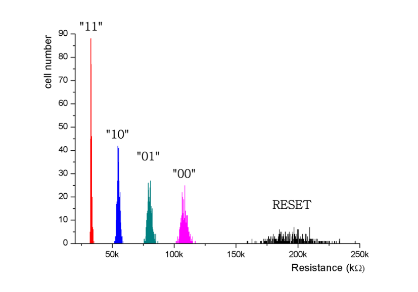 Fig.13: RON and ROFF distributions versus cell variability (σVariability = 15%) after 300 runs (SET and RESET states)
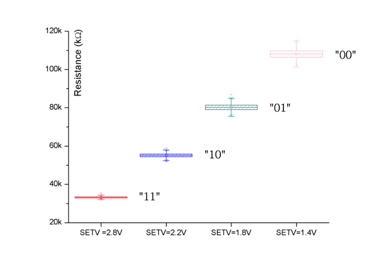 Fig.14: RON distribution box-plots versus cell variability (σVariability = 15%) after 300 runs (SET states)
To evaluate the robustness of the technology, Figure 15 and Figure 16 results are provided for σVariability = 20% and σVariability = 25%, which is the worst case. An important spreading of RON is observed. The initial RON distribution spread increases as variability increase. Even for the worst case (σVariability = 25%), no overlap between LRS distributions is observed which confirms the robustness of MLC approach. In Table 5, RON (SET) and ROFF (RESET) distribution parameters (mean value and standard deviation) are reported for the different variability parameter values.
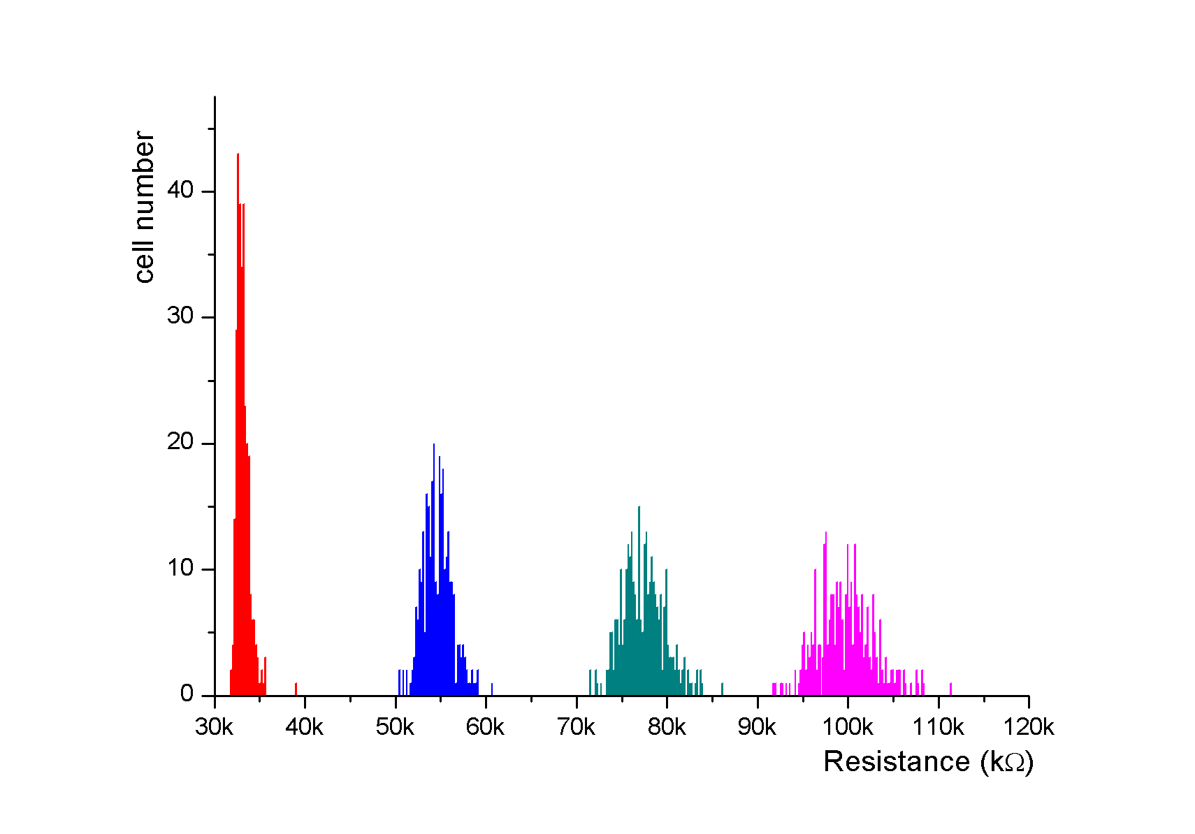 Fig.15: RON distributions versus cell variability (σVariability = 20%) after 300 runs (SET states)
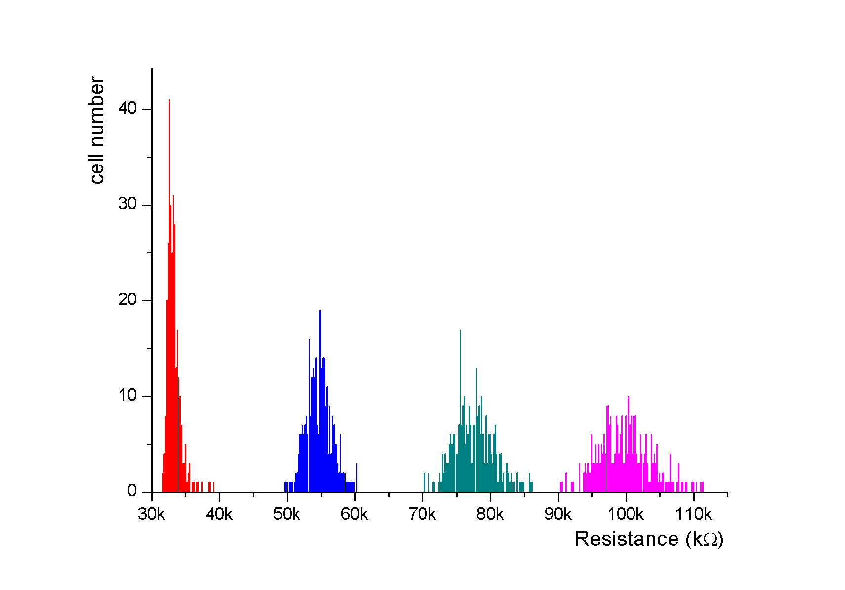 Fig.16: RON distributions versus cell variability (σVariability = 25%) after 300 runs (SET states)
Table 5: Simulated Configurations
| SET | RESET | |||||
| σVariability | Distributions | 11 | 10 | 01 | 00 | |
| 15% | Mean (kΩ) | 33.159 | 55.111 | 80.227 | 108.119 | 195.350 |
| σ (kΩ) | 0.501 | 1.153 | 1.8550 | 2.5520 | 14.447 | |
| 20% | Mean (kΩ) | 33.239 | 54.681 | 77.402 | 99.672 | 196.639 |
| σ (kΩ) | 0.768 | 1.614 | 2.408 | 3.174 | 19.520 | |
| 25% | Mean (kΩ) | 33.342 | 54.761 | 77.529 | 99.844 | 198.031 |
| σ (kΩ) | 1.049 | 1.973 | 2.978 | 3.928 | 24.882 | |
5. Conclusion
Variability combined with voltage drops due to resistive paths present a major challenge for ReRAM memory fabrication process and design engineers. In the proposed study, impact of variability combined with resistive paths is evaluated based on a 1T1R ReRAM elementary memory array. A specific attention is provided to the ReRAM memory word. To assess the technology reliability, the HRS/LRS resistance ratio is extracted at a memory word and at a memory array level to provide a valuable feedback for designers during ReRAM memory array design. At a word level, impact of line resistances combined with variability can affect the memory word operation from a word size greater than 8 bits. At a memory array level, resistance variability in RESET state is much more important than variability in the SET state. Additionally, a stable MLC operation of 2-bits/cell is demonstrated.
- Aziza, P. Canet, J. Postel-Pellerin, M. Moreau, JM. Portal, M. Bocquet, “ReRAM ON/OFF resistance ratio degradation due to line resistance combined with device variability in 28nm FDSOI technology”, Ultimate Integration on Silicon (EUROSOI-ULIS), 2017. DOI: 10.1109/ULIS.2017.7962594.
- Semiconductor Industry Association, “International Technology Roadmap for Semiconductors”.
- Shahrabi, B. Attarimashalkoubeh, J. Sandrini, and Y. Leblebici, “Towards chip-level reram-cmos co-integration”, in International Conference on Memristive Materials, Devices and Systems (MEMRYSIS), 2017. DOI: 10.1109/PRIME.2016.7519497.
- Aziza, H. Ayari, S. Onkaraiah, M. Moreau, JM. Portal, “Multilevel operation in oxide based resistive RAM with SET voltage modulation”, in International Conference on Design and Technology of Integrated Systems in nanoscale Era, 2016. DOI: 10.1109/DTIS.2016.7483892.
- Waser, R., Nanoelectronics and Information Technology: John Wiley & Sons, 2012.
- Chen, F., Seok, J.Y. and Hwang, C.S., Integration Technology and Cell Design, in Resistive Switching, Wiley-VCH Verlag GmbH & Co. KGaA, 573-596, 2016. DOI: 10.1002/9783527680870.ch20.
- Molas, G., et al. “Functionality and reliability of resistive RAM (RRAM) for non-volatile memory applications.” 2016 International Symposium on VLSI Technology, Systems and Application (VLSI-TSA). IEEE, 2016. DOI: 10.1109/VLSI-TSA.2016.7480520.
- Liang & al., “Effect of wordline/bitline scaling on the performance, energy consumption, and reliability of cross-point memory array”, ACM Journal on Emerging Technologies in Computing Systems, Vol. 9, No. 1, 2013. DOI: 10.1145/2422094.2422103.
- I. Vatajelu et al., “Nonvolatile memories: Present and future challenges”, Design & Test Symposium (IDT), 61-66, 2014. DOI: 10.1109/IDT.2014.7038588.
- Hyo-Shin Ahn1 et al., “Pairing of cation vacancies and gap-state creation in TiO2 and HfO2,” Phys. Lett., Vol. 90, Iss. 25, p. 252908 – 252908-3 (2007). DOI: 10.1063/1.2749858.
- Lien et al., “The highly scalable and reliable hafnium oxide ReRAM and its future challenges”, Solid-State and Integrated Circuit Technology (ICSICT), 2010. DOI: 10.1109/ICSICT.2010.5667553.
- Bocquet et al., “Compact Modeling Solutions for Oxide-Based Resistive Switching Memories (OxRAM)”, Journal of Low Power Electronics and Applications, 4 (1), 1-14, 2014. DOI: 10.1109/FTFC.2013.6577779.
- Mazure, et al., “FDSOI: From substrate to devices and circuit applications”, ESSCIRC, 45-51, 2010. DOI: 10.1109/ESSCIRC.2010.5619767.
- Nardi, et al, “Resistive switching by voltage-driven ion migration in bipolar RRAM Part I: Experimental study”, IEEE Transactions on Electron Devices, 59(9), 2461-2467, 2012. DOI: 10.1109/TED.2012.2202319.
- Larentis, et al., “Resistive switching by voltage-driven ion migration in bipolar RRAM Part II: Modeling”, IEEE Trans. on Electron Devices, 59(9), 2468-2475, 2012. DOI: 10.1109/TED.2012.2202320.
- Diokh, “Investigation of the Impact of the Oxide Thickness and RESET conditions on Disturb in HfO2-RRAM integrated in a 65nm CMOS Technology” in International Reliability Physics Symposium, 3-6, 2013. DOI: 10.1109/IRPS.2013.6532043.
- C. Huang et al., “Using binary resistors to achieve multilevel resistive switching in multilayer NiO/Pt nanowire arrays”, NPG Asia Materials, 6 (2), e85, 2014. DOI:10.1038/am.2013.81.
- S. Fan et al., “High Endurance and Multilevel Operation in Oxide Semiconductor-Based Resistive RAM Using Thin-Film Transistor as a Selector”, ECS Solid State Letters, 4(9), Q41-Q43, 2015. DOI: 10.1149/2.0061508ss.