Design and Simulation of an RF-MEMS Switch and analysis of its Electromagnetic aspect in realtion to stress

Adv. Sci. Technol. Eng. Syst. J. 3(1), 76–81 (2018);
 DOI: 10.25046/aj030109
Microelectromechanical Systems (MEMS) are devices made up of several electrical and mechanical components. They consist of mechanical functions (sensing, thermal, inertial) and electrical functions (switching, decision making) on a single chip made by microfabrication methods. These chips exhibit combined properties of the two functions. The size of system has characteristic dimensions less than 1mm but more than 1mm. The configuration of these components determine the final deliverables of the switch. MEMS can be designed to meet user requirements on any level from microbiological application such as biomedical transducers or tissue engineering, to mechanical systems such as microfluidic diagnoses or chemical fuel cells. The low cost, small mass and minimal power consumption of the MEMS makes it possible to readily integrate to any kind of system in any environment. MEMS are faster, better and cheaper. They offer excellent electrical performances. MEMS working at Radio frequencies are RF MEMS. RF-MEMS switches find huge market in the modern telecommunication networks, biological, automobiles, satellites and defense systems because of their lower power consumptions at relatively higher frequencies and better electrical performances. But the reliability is the major hurdle in the fate of RF MEMS switches. Reliability mainly arises due to the presence of residual stresses, charging current, fatigue and creep and contact degradation. The presence of residual stresses in switches the S-Parameters of the switches are affected badly and the residual stress affects the final planarity of the fabricated structure. Design and simulation of an RF-MEMS switch is proposed considering the residual stresses in both on and off state. The operating frequency band is being optimized and the best possible feasible fabrication technique for the proposed switch design is being analyzed. S-Parameters are calculated and a comparison for the switches with stress and without stress is performed in FEM based HFSS software.
1. Introduction
MEMS technologies are faster, better, and cheaper. They have reduced size and weight, means fewer power consumption and there are lower component counts. MEMS promises superior electrical performances and are built with low cost [1]. They can be produced at massive level. They have advanced functionality and superior reliability. They have new functionality and better system capability.
The ultimate goals of MEMS are to reduce size, cost, weight, power consumptions by increasing the performance of existing macroscopic devices [2]. To make devices never before possible at macroscopic scale. Easy to integrate into systems or modify. They have Small thermal constant and they can be highly resistant to vibration, shock and radiation. MEMS are Microelectro- mechanical system in which the device and structures are fabricated at micro levels using the micro level fabrication process [3]. It is basically an integrated micro devices or systems combining electrical and mechanical components fabricated using Integrated Circuit (IC) compatible processing technique and it range from micron to millimeter [4].
MEMS structures can be a simple system with all static elements or large complicated system with some parts moving and some static elements. Chief concept of MEMS is that there is at least one moving element [5]. MEMS most important elements are micro sensors and micro actuators. Basically these are the transducers that convert electrical to mechanical and vice versa. Micro actuators and micro sensors are widely used in the integrated circuits industry due to low per device cost and other benefits.
2. Radio Frequency MEMS
2.1. Maintaining the Integrity of the Specifications
MEMS can be classified into different types depending upon their mean of actuation. These include acoustic MEMS, optical MEMS and Radio Frequency MEMS (RF-MEMS) [6]. RF MEMS operate in the electromagnetic wave frequencies in the 3 kHz – 300 GHz range [7-8]. This frequency provides maximized efficiency in the circuitry and ability to flow through paths containing insulating material, such as the dielectric insulators of capacitors.
3. Microfabrication of RF-MEMS Switch and Thermal Induction of Residual Stress
In Trento Italy; at ITC-IRST research center; using gold electroplating a process was carried out on micro bridge and RF MEMS; which resulted in obtaining suspended microstructure by photoresist of 3micrometer thickness [2].
3.1. RF Switch Surface (RFS) Micromachining
The RF-MEMS STS whose design is considered in this study is realized through the gold electrodeposition microfabrication
- At 975C in a wet atmosphere silicon wafer came in contact with thermal oxide of 1000nm thickness and then with nitrogen. Resistors and lines are formed by polysilicon while pattern is formed by dry ditching
- At 718C silicon oxide is placed with wafer and after that applied to photolithography.
- A metal is spitted for signal line generation. The general temperature is 400C but when LPCVD oxide is deposited temperature rises by 30C. The area which was free from photoresist; for electrical contact oxide is removed by dry etching then wafer is washed.
- Wafer is now wet etched and floating metal (Cr/Au) layer is evaporated. 3micrometer thickness of Cr is placed between oxide layer and Au.
- At 52C electroplating of gold on seed layer is done.
- At 52C; gold layer is used for strengthen the structure. It’s left for 30 minutes a 190C. Finally at 200C structure comes
in contact with plasma oxygen for removing extra layers.
3.2. Mechanisms contributing to Residual Stress Induction
For residual stress following steps are made: –
1. Stress In this process; Cr-Au PVD is deposited on photoresist. Seed layer is used for ensuring adhesive property of Au. Although due to thermal instability chromium oxide is formed along with residual stress.
2. Gradient happens due to difference in thermal coefficient of gold and seed layer. Seed layer expands more rapidly and results in tensile residual stress. However micro beams get deformed due to release of Au.
3. Oxygen Plasma ashing helps in avoiding sticking but temperature changes too rapidly forming residual stress. Temperature is maintained at 200C so that Au reached even the narrow paths.
4. Design of RF-MEMS Symmetric Toggle Switches
4.1. On State without stress
The simply designed switch in HFSS is the extension of work presented in “Simulating the Electromagnetic Effects of Thermally Induced Residual Stresses in RF-MEMS Switches”. This RF-MEMS switch is designed in FEM based HFSS software. In this switch, (Figure 1) simply a suspended type bridge was designed over the coplanar waveguide transmission line, the design of the switch is as follow. The gold material was assigned to the bridge, this switch was designed just to ensure the results validity with the already present standards in the literature.
Similarly, when the stress was induced in the switch, (Figure 2) the central bridge of the switch deflected upward, which ultimately affected the overall electromagnetic performance of the switch.
4.2. Identify the Headings Design of a simple RF-MEMS Switch in off-state without stress
When the switch is in the off state, the bridge deflects downwards at the center just over the dielectric layer of signal CPW (Figure 3). The side conductors of the CPW are grounded while the signal pass through the central conductor of CPW
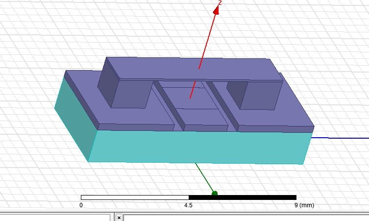 Figure 1: Design of a simple RF-MEMS Switch without stress and excitation
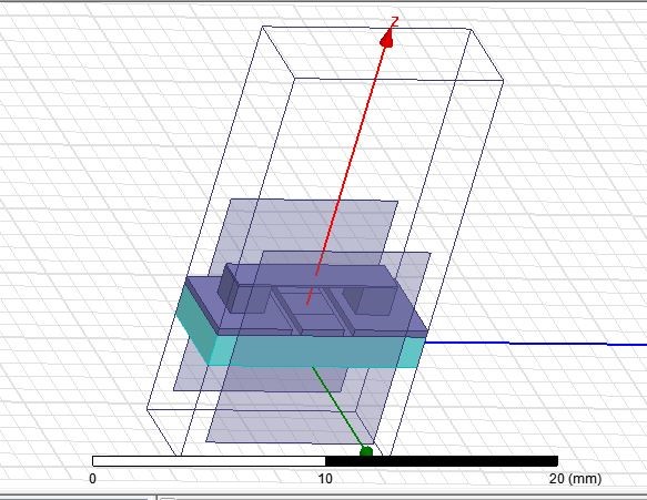 Figure 2: Design of a simple RF-MEMS Switch without stress and excitation and air box
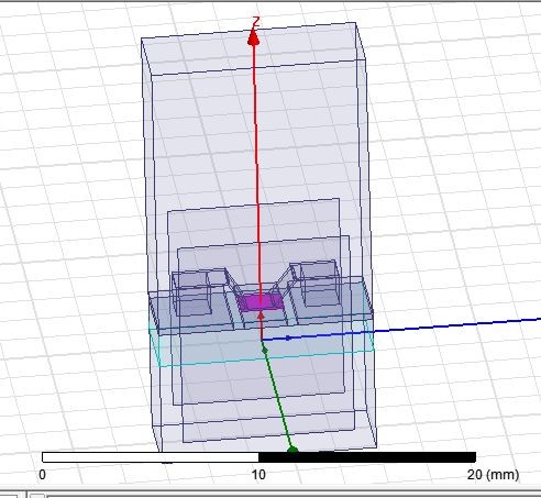 Figure 3: Design of a simple RF-MEMS Switch in off-state without stress
The excitation of the switch is applied through waveport excitations and it is shown in the figure as red shaded side conducting sheet. The waveport connects the central conductor of the CPW with the side conductors, and are used to supply the signal through the switch (Figure 4).
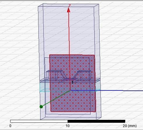 Figure 4: Design of a simple RF-MEMS Switch in off-state without stress with the excitation shown
5. Comparison of simply designed switch with the results already present in literature
5.1. Return Loss of On State
Per the Rangra at Kamal and Jacobi [9], the reflection coefficient of the switch during the on state must be always less than -10 dB, which ensures better switch performances. When we designed a simple switch RF-MEMS switch in HFSS software, the result of reflection coefficient was ascending curve along the X-axis. The result of this switch (Figure 5) is exactly in accordance with existing standards of literature [10, 11] which ensures that our approach was accurate.
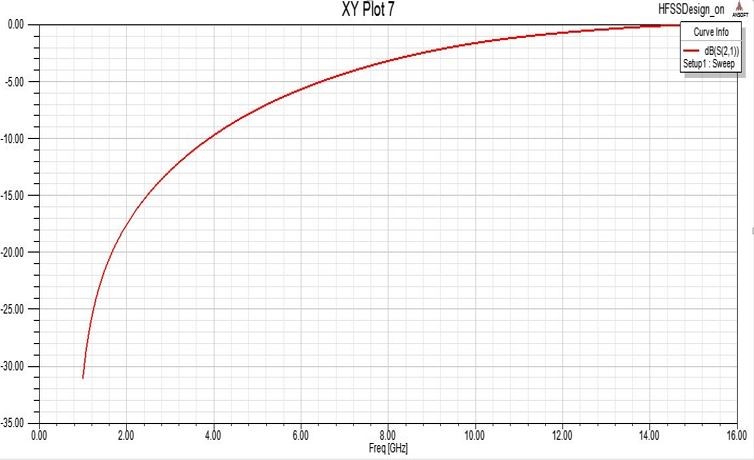 Figure 5: Simulated results of on state return loss
As shown in the graph above, at lower frequencies like between 1.5 GHz to 4 GHz, the reflection was good. Later as the operating frequency range increased, the switch moved to lesser matching or the reflection of the power from the switch increased. From the frequency range of 8GHz to 16 GHz, the switch was not in ideal conditions i.e. the refection increased at higher frequencies. The result already stated in literature (Figure 6) also showed the same trend as shown below [10, 12]. The reflection increased as we move on to higher frequencies.
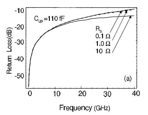 Figure 6: Literature results of on state return loss [2, 10]
5.2. Insertion loss of on state
Ideally, the switch during the on state should have minimum insertion loss, i.e. the value of transmission coefficient should be zero or close to zero. The results which we obtained for a simple RF-MEMS switch in the on state are shown in the graph below, here as the frequency increases, the value of transmission coefficient increases, which predicts lower or poor insertion loss (Figure 7). Ideally the transmission coefficient should be zero as state hypothetically in the literature (Figure 8), but in actual it is not possible to have perfectly zero transmission coefficient [2, 10]. But as the frequency increases, overall there is a decline in the value of transmission coefficient. Which means that at higher frequencies the transmission reduces [13].
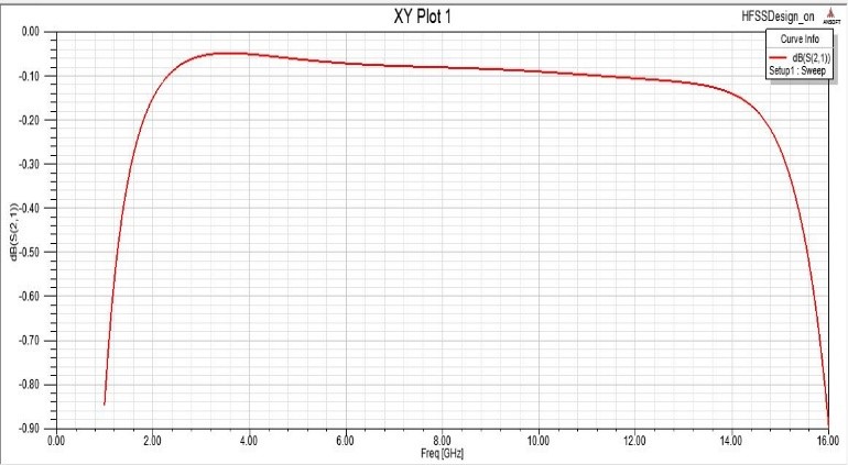 Figure 7: Simulated results of on state Insertion loss
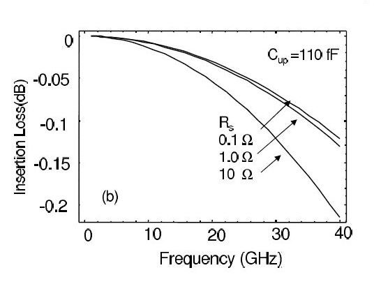 Figure 8: Literature results of on state Insertion loss [2, 10]
5.3. Return Loss of Off-State
Now when the switch is in off-state, the value of reflection coefficient should be greater than -10 dB because at the off-state, switch is not in the working conditions. Maximum power which is incident to the switch gets reflected back [14]. So as the literature predicts, if the operating frequency is taken on X-axis and the transmission coefficients along Y-axis, then the graph should be an ascending curve. So our results of a simple RF-MEMS switch (Figure 9) were found to be exactly similar to those, which were mentioned in the literature (Figure 10). The slight difference in the curve can be explained in terms of the operating frequency ranges i.e. in our graph the limit was between 0 GHz to 16 GHz, whereas in the standard the limit was between 0 GHz to 40 GHz.
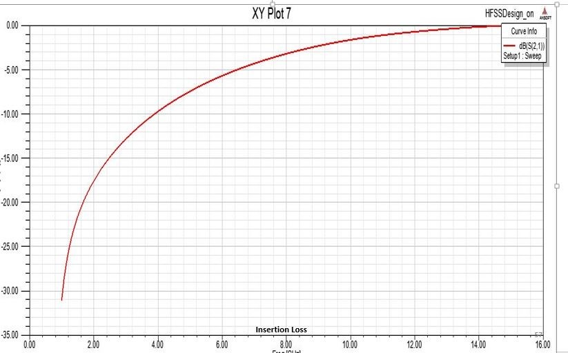 Figure 9: Simulated results of off state return Lost
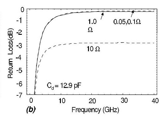 Figure 10: Literature results of off state return Loss. [2, 10]
5.4. Result of Isolation in Off State
According to the set standards, the isolation should be maximum in the off-state. Due to higher isolation, the leakage of power during off-state is minimum [15]. The S21 represents the isolation in the off-state. So, here the curve according to the set standard is descending curve, followed by a dip at nearly 15 GHz, and then a gradually ascending curve, after 15 GHz. So, our results of the simple RF-MEMS switch (Figure 11) are in accordance with the pre-defined standards (Figure 12). So, maximum isolation was observed at off-state nearly at 15 GHz.
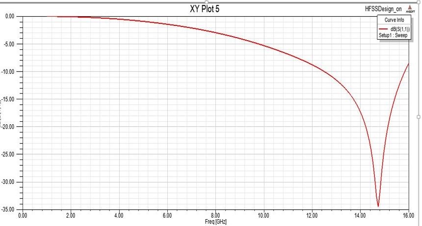 Figure 11: Simulated results of off state Isolation
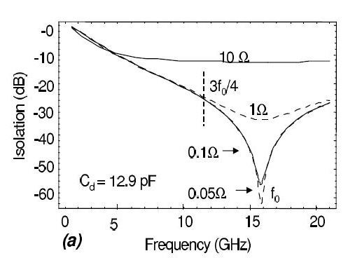 Figure 12: Literature results of off state Isolation. [2, 10]
6. ANALYSIS OF RESULTS
6.1. Without stress
The value of return loss S11 in the RF-MEMS switch without stress, shows excellent results. The value of reflection coefficients is much less than -10 dB, which indicates the best matching in the sense of transmitting power. The value of S11 lies between -58 dB to -42 dB, which indicates the very less power is reflected. As the value is much lesser than -10 dB, so we can say that switch is having excellent matching or very good reflection loss [16, 17]. Ideally any operating switch must have, reflection loss less than -10 dB, then it is assumed that the electrical performance of the switch is better. If any switch does not have this predefined reflection coefficient, then it means that maximum of the power is wasted or reflected back rather than transmitting through the switch [18]. So, the designed switch in HFSS software, which was already fabricated showed excellent electrical performance in the on state. Their electromagnetic performances are good for the frequency ranges between 2GHz to 16 GHz but, are best between the frequencies of 1.5 GHz to 8GHz. Similarly, the value of transmission coefficient is near 0dB, which means that overall transmission through the switch is excellent. The logic behind stating this is that as we know 0dB is actually equal to 1. It means when the value of transmission is or close to 0dB then the transmission through the switch will be excellent. Again, the operating frequency ranges between 1GHz to 8GHz. Because as the frequency increases, the transmission decreases.
6.2. With Stress
Due to the generation of residual stresses in the RF-MEMS switch, the reflection of the switch is badly affected. The reason is that due to generation of stresses, the bridge deflects upward at the center. Now the air gap between the top central bridge and the ground dielectric increases [19, 20, 21]. Due to rise in air gap the up-state capacitance of the switch is decreased now. As we already explained in the design aspect of RF-MEMS switch that S-parameters are dependent upon the up and down state capacitances. Reflection is dependent upon the up-state capacitances while the isolation is affected by down state capacitances [22, 23, 24]. The results of return loss with stress are shown in Figure 13.
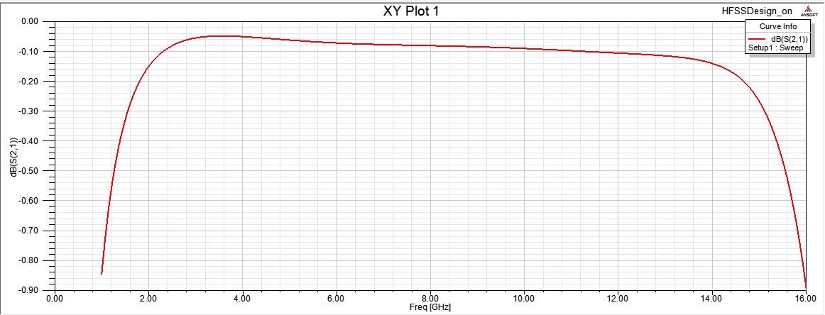 Figure 13: Simulated results of return loss with stress
Similarly, the results for insertion loss are shown in Figure 14.
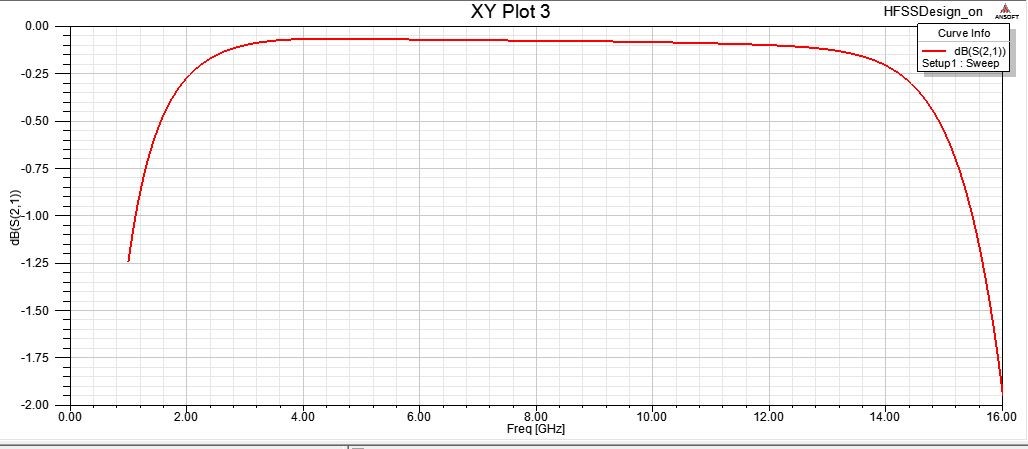 Figure 14: Simulated results of insertion loss with stress
7. Conclusion
So we can conclude that switch was operating efficiently when there were no residual stresses but due to the generation of residual stresses, not only the final planetary of the switch was affected but also the electrical performance of the switch was affected badly. Future work can be done on how to reduce the residual stresses in RF-MEMS switch during microfabrication when the temperature is changed abruptly. Some research can also be produced in the domain of improving reliability of RF-MEMS switches by reducing the effects of charging of dielectric, the effects of creep and fatigue along with the contact degradation. So that it may help to improve the overall efficiency of the RF-MEMS switch.
- G. Rebeiz, K. Entesari, I. Reines, S. J. Park, M. El-tanani, A. Grichener, and A. Brown, “Tuning in to RF MEMS”, Microwave Magazine, IEEE, vol. 10, no. 6, pp. 55-72, 2009.
- Solazzi F, Margesin B and Faes A, “Novel Design Solutions for High Reliability RF MEMS Switches”, 2010
- R. Osiander, M. A. G. Darrin, and J. L. Champion, MEMS and Microstructures in Aerospace Applications. New York, NY, USA: Taylor & Francis, 2006.
- G. M. Rebeiz, RF MEMS: Theory, Design, and Technology. John Wiley & Sons, Inc., 2003.
- N. Barker and G. Rebeiz, “Optimization of distributed MEMS transmission-line phase shifters-U-band and W-band designs,” Microwave Theory and Techniques, IEEE Transactions on, vol. 48, no. 11, pp. 1957 – 1966, Nov. 2000.
- A. Verger, A. Pothier, C. Guines, A. Crunteanu, P. Blondy, J. Orlianges, J. Dhennin, F. Courtade, and O. Vendier, “Sub-hundred nanosecond reconfiguration capabilities of nanogap RF MEMS switched capacitor,” in Microwave Symposium Digest (MTT), 2010 IEEE MTT-S International, May 2010, pp. 1238 -1241.
- H. Newman, J. Ebel, D. Judy, and J. Maciel, -Lifetime Measurements on a High-Reliability RF-MEMS Contact Switch,” Microwave and Wireless Components Letters, IEEE, Feb 2008.
- Mulloni J, Giacomozzi V and Margesin B 2010 Controlling stress and stress gradient during the release process in gold suspended micro-structures Sensors Actuators A 162 93-9.
- B. Pillans, J. Kleber, C. Goldsmith, and M. Eberly, “RF power handling of capacitive RF MEMS devices,” in Microwave Symposium Digest, 2002 IEEE MTT-S International, 2002.
- J. Muldavin, C. Bozler, S. Rabe, P. Wyatt, and C. Keast, “Wafer- Scale Packaged RF Microelectromechanical Switches,” Microwave Theory and Techniques, IEEE Transactions on, vol. 56, no. 2, pp.522 -529, 2008.
- A. Grichener and G. Rebeiz, “High-Reliability RF-MEMS Switched Capacitors With Digital and Analog Tuning Characteristics,” Mi-crowave Theory and Techniques, IEEE Transactions on, vol. 58, no. 10, pp. 2692 -2701, 2010.
- B. Lakshminarayanan, D. Mercier, and G. Rebeiz, “High-Reliability Miniature RF-MEMS Switched Capacitors,” Microwave Theory and Techniques, IEEE Transactions on, vol. 56, no. 4, pp. 971 -981, 2008.
- D. Mardivirin, A. Pothier, A. Crunteanu, B. Vialle, and P. Blondy, “Charging in Dielectricless Capacitive RF-MEMS Switches,” Microwave Theory and Techniques, IEEE Transactions on, vol. 57,no. 1, pp. 231 -236, 2009.
- T. Rijks, J. van Beek, P. Steeneken, M. Ulenaers, J. De Coster, and R. Puers, “RF MEMS tunable capacitors with large tuning ratio,” in17th IEEE International Conference on. MEMS, 2004.
- F. Casini, P. Farinelli, G. Mannocchi, S. DiNardo, B. Margesin, G. De Angelis, R. Marcelli, O. Vendier, and L. Vietzorreck, “High Performance RF-MEMS SP4T switches in CPW technology for space Applications”, in Microwave Conference (EuMC), 2010 European, 2010, pp. 89 -92.
- I. Reines, S. J. Park, and G. M. Rebeiz, “Compact Low-Loss Tunable Band Bandstop Filter With Miniature RF-MEMS Switches,” Microwave Theory and Techniques, IEEE Transactions on, vol. 58, no. 7, pp. 1887 -1895, 2010.
- A. Ocera, P. Farinelli, F. Cherubini, P. Mezzanotte, R. Sorrentino, B. Margesin, and F. Giacomozzi, “A MEMS-Recon_gurable Power Divider on High Resistivity Silicon Substrate,” in Microwave Symposium, 2007. IEEE/MTT-S International, 2007, pp. 501 -504.
- M. Kim, J. Hacker, R. Mihailovich, and J. DeNatale, “A DC-to-40 GHz four-bit RF MEMS true-time delay network,” Microwave and Wireless Components Letters, IEEE, vol. 11, no. 2, pp. 56 -58, Feb.2001.
- T. Vaha-Heikkila, J. Varis, J. Tuovinen, and G. Rebeiz, “A 20-50 GHz RF MEMS single-stub impedance tuner,” Microwave and Wireless Components Letters, IEEE, vol. 15, no. 4, pp. 205 – 207, 2005.
- Rebeiz G M 2003 RF MEMS: Theory, Design and Technology (New York: Wiley)
- W. Auer, E. Hettlage, and G. Ru_, “RF-switches: Application and design,” in ESA, Proceedings of the 3rd European Space Mechanisms and Tribology Symposium p 191 -195 (SEE N88-21191 14-18), Dec.1987, pp. 191-195.
- R.C. Hibbeler, “Mechanics of Materials”, Edition 9, pp 153
- Fang W, Lee C H and Hu H H 1999 On the buckling behavior of micromachined beams J. Micromech. Microeng.9 236–44