Impact of Crosstalk on Signal Integrity of TSVs in 3D Integrated Circuits

Adv. Sci. Technol. Eng. Syst. J. 3(1), 109–114 (2018);
 DOI: 10.25046/aj030113
Through-Silicon-Vias (TSVs) are utilized for high density 3D integration, which induce crosstalk problems and impact signal integrity. This paper focuses on TSV crosstalk characterization in 3D integrated circuits, where several TSV physical and environmental configurations are investigated. In particular, this work shows a detailed study on the influence of signal-ground TSV locations, distances and their structural configurations on crosstalk. Embedded 3D testing circuits are also presented to evaluate the coupling effects between adjacent TSVs such as crosstalk induced delay and glitches for different crosstalk modes. Additionally, A 3D parallel Ring Oscillators testing structure is proposed to provide crosstalk strength coupling indicator between adjacent TSVs. Simulation results are conducted using a 3D electromagnetic field solver (HFSS) from Ansoft Corporation and a Spice-like simulator (ADS) from Keysight Technologies Corporation based on MIT 0.15µm 3DFDSOI process technology.
1. Introduction
3D Interconnect is the promising technology [1]-[4], which includes Through-Silicon-Vias (TSVs) to connect vertically stacked semiconductor chips with shortest paths, which means lowest inductance and conduction loss, to both signals and power supplies. In spite of these benefits, the signal integrity issues in TSVs become the major challenges in 3D designs [5-6]. The goal of TSVs or 3D Vias development is to acquire high chip density. Therefore, the density of the 3D Vias is also high. In this environment, a crosstalk problem appears between two adjacent signal 3D Vias (Aggressor and Victim). Studies show that the coupling problem is not negligible in TSVs because of the relatively large diameter and small pitch, which results in non-negligible TSV-to-TSV coupling that degrades significantly the 3D circuit performance. Hence, it becomes very essential to precisely model and evaluate the electrical characteristics of TSVs [7]-[9] to analyze signal integrity (SI), and crosstalk of adjacent TSVs under the conditions of various structures and configurations.
In this paper, the electrical characteristics of 3D interconnect, based on our previous work [10], is presented to characterize signal integrity effects of 3D crosstalk for different TSVs placement and configurations. 3D Vias based on 0.15 µm 3DFDSOI process from MIT Lincoln lab [11] are used as a device under test (DUT) for crosstalk characterization where a 3D full wave simulator such as HFSS from Ansoft Corporation is used to extract and predict the electrical characteristics of TSVs in the frequency domain (S-Parameters) and a Spice-like simulator such as ADS from KEYSIGHT technologies to evaluate the TSVs transient response in the time domain (Eye-diagram). Additionally, embedded 3D testing applications are proposed to characterize the TSV’s signal integrity effects and the impact of TSVs on the 3D circuit performance after fabrication. A 3D circuit test is presented to evaluate the coupling effects between adjacent TSVs such as induced-delay and glitches [12-13] for different crosstalk modes. Additionally, a consecutive triggered parallel Ring Oscillators (ROs) testing structure is proposed to provide a crosstalk coupling indicator between adjacent TSVs.
The paper is organized as follows: section 2 discusses the 3D Full wave modeling for TSV and the simulation setup. A detailed study of crosstalk for different physical and environmental TSVs configurations is given in Section 3. 3D Crosstalk embedded testing applications are given in Section 4. Section 5 concludes the paper.
2. A 3D Full Wave Modeling for TSVs
In order to evaluate the electrical characteristics of a TSV depending on structural parameters such Via pitch, Via height, and Via size, the 3D interconnect based on MIT 0.15µm 3DFDSOI technology is used as DUT to model and characterize crosstalk in different testing configurations. The vertical connection in this technology is slightly different from the standard Through-Silicon-Via (TSV), which is a square shape via made from Tungsten material and fully surrounded by oxide; thus, it is simply called a 3D Via. The 3D Via pitch is around 3.325 µm (distance between the centers of two 3D Vias), 7.34 µm TSV height, 1.25 µm x 1.25 µm TSV size. The physical size of 3D Via after fabrication is estimated to be around 2 µm for the top dimension and 1 µm for the bottom dimension. The 3D Via was simulated using a 3D full wave simulator (HFSS from Ansoft Corporation), which generates the S-Parameters of the structural model of the Via and a Spice type simulator (ADS from Keysight Corporation) to predict the electrical characteristics of 3D Vias in the time domain (Eye-diagram). Figure 1 presents a pair of TSVs structure using the HFSS simulator.
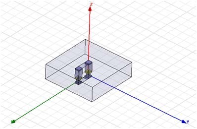 Figure 1. Physical Structure of a pair of TSVs using 3D full wave simulator
Usually, an interconnection line is characterized using S-Parameters. S11 and S21 are the S-parameters reflection and transmission coefficients respectively, which are typical characteristics of an interconnection. The evaluated S11 and S21 magnitudes for the electrical characteristics of a 3D Via based on the default parameters are shown in Figure 2.
The transmitted data stream through the 3D Via was simulated with the evaluated S-parameters from the 3D full wave simulator (HFSS). The Eye-diagram of the transmitted data stream was evaluated for 107-1 pseudo random bits sequence (PRBS) using the Spice type circuit simulator (ADS). The source for the simulation has 1.5 Vp-p and 50Ω source termination. The 3D Via is terminated by a shunt connected 50 Ω resistor and 1pF capacitor. The Eye-diagrams of 2 Gbps, and 10 Gbps PRBSs are shown in Figure 3. Also, all PRBSs were assumed that they have 10% rising and falling times
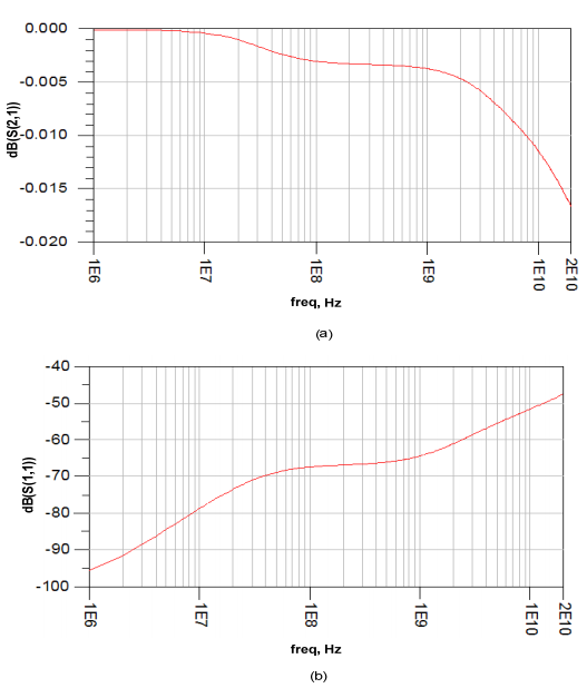 Figure 2. Evaluated S21 magnitude (a) and S11 magnitude (b) of 3D via using HFSS
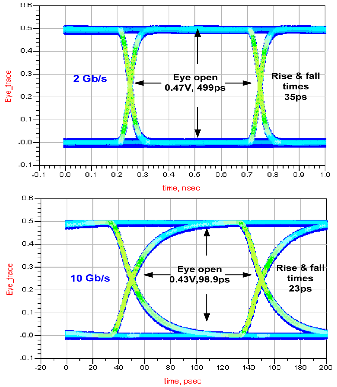 Figure 3. The simulated eye-diagrams of 2Gbps (a), and 10 Gbps (b) PRBSs after passing through the 3D Via
3. A Crosstalk between 3D Vias
3.1. The Influence of 3D Via Locations, and Distances on Crosstalk
Crosstalk is evaluated depending on the distance of two signal Vias and the location of two GND Vias as shown in Figure 4.
Five distances (4 µm, 8 µm, 16 µm, and 32 µm) based on SGSG configuration between the two signal Vias have been simulated. As expected, if the distance between the two signal 3D Vias is larger, the crosstalk level is going down as shown in Figure 5. The effect of the distance of GND Vias with respect to the signal via on the crosstalk is also evaluated as shown in Figure 6 with four distances: 4 µm, 8 µm, 16 µm, and 32 µm. The results show an increase in the magnitude of the crosstalk as the distance of the reference via (GND) increases. Also it is shown in Figure 7 that the crosstalk magnitude of SGGS (i.e. the cross locations of the signal and ground Vias) configuration is smaller than that of SGSG configuration comparing two same distance cases. The difference of the two cases is almost 10dB. This is a very interesting point for 3D designers to keep in mind, because just changing the 3D Via role can reduce the crosstalk magnitude especially in high frequency applications, where crosstalk problem is very critical to obtain the maximum system performance.
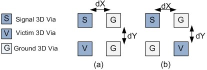 Figure 4. Location of signal Vias and GND Vias for crosstalk evaluation, (a) SGSG, (b) SGGS configurations
 Figure 5. Comparison of five locations of 3D Vias. The distances 4 µm, 8 µm, 16 µm, and 32 µm between two signal Vias are associated to the graphs from top to bottom respectively
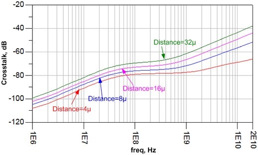 Figure 6. Comparison of three locations of GND Vias. The distances 4 µm, 8 µm, 16 µm, and 32 µm between two GND Vias are associated to the graphs from bottom to top respectively
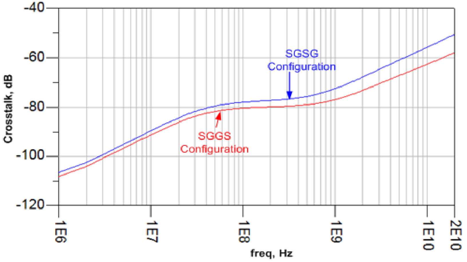 Figure 7. Comparison between SGSG and SGGS configurations for 10 µm distance, SGSG and SGGS are the top and bottom graphs respectively
3.2. 3D Via Crosstalk in Structures with Different Configurations
The geometry of the return current path may be one of the most efficient methods to affect the crosstalk between a signal and victim Via. Four different configurations have been investigated (1) Two Via pairs in a straight line (Figure 8(a)), (2) Two Via pairs placed opposite to each other (Figure 8(b)), (3) A signal Via with two reference via placed opposite to a victim Via with two ground Vias (Figure 8(c)), (4) A signal and victim via, each with three reference Vias as a return current path (Figure 8(d)).
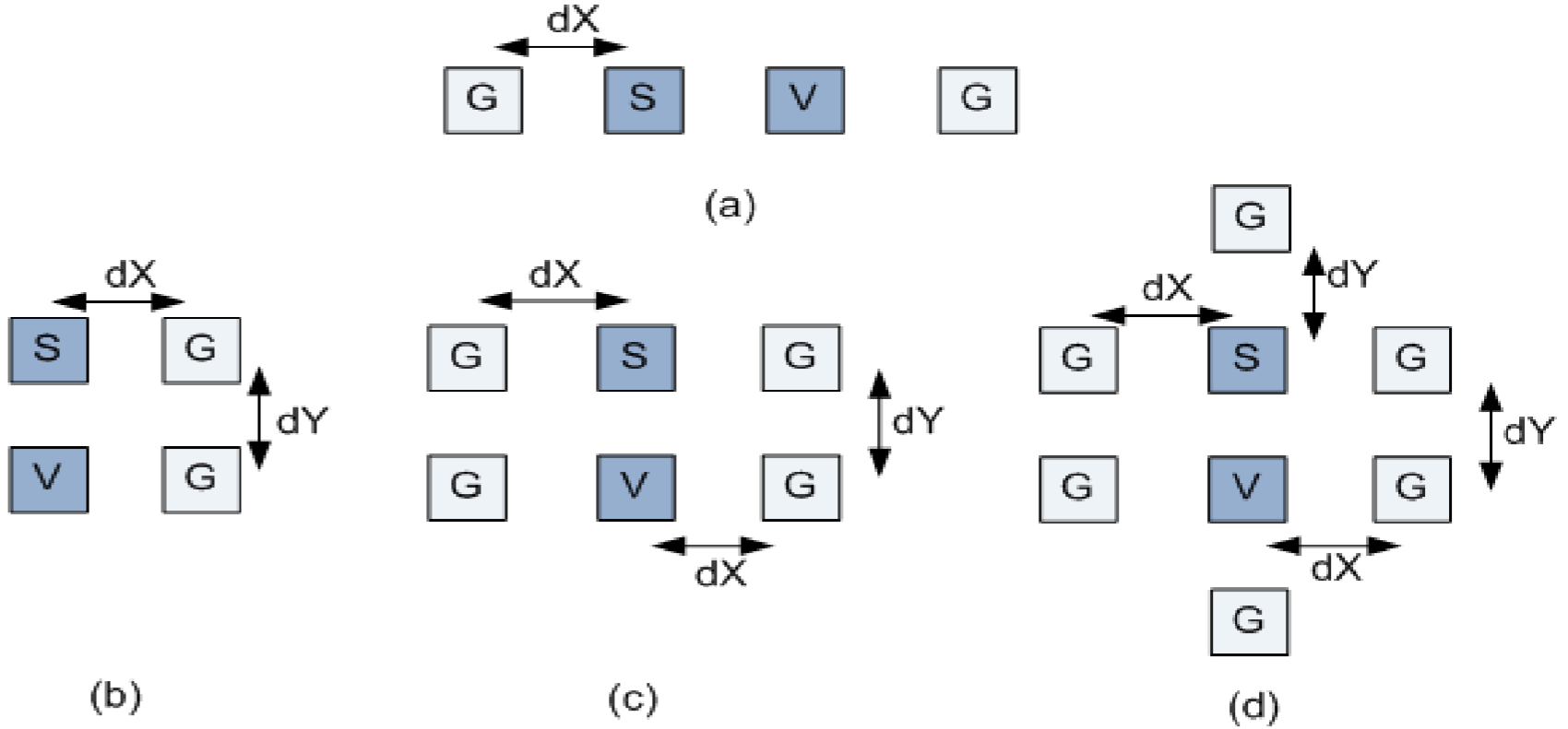 Figure 8. Comparison of three different configurations, (a) Configuration #1, (b) Configuration #2, (c) Configuration #3, and (d) Configuration #4
In configuration 2, the signal Via has a slightly lower inductance than it would in configuration 1 because the second Via is close enough to the signal Via to have a slight impact on its inductance. Configuration 4 has the lowest inductance because it has the most well defined return current path. This lowering of the inductance will also lower the near-end crosstalk as shown in Figure 9. Also it is shown that the highest crosstalk as predicted, comes from configuration 1. Only slightly lower is the crosstalk from configuration 2. Then, there is a significant decrease in crosstalk when the extra two reference Vias are added in configuration 3, and a slight decrease further when the third reference Via is added to the victim and signal Vias in configuration 4. The reduction in crosstalk from adding additional reference Vias is almost 4 dB.
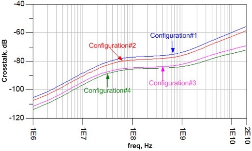 Figure 9. Crosstalk between four different configurations
Until this point, only isolated 3D Vias with respect to ground Vias have been considered. Potential coupling in the 3D Vias in the discontinuity between the 3D via and the transmission line may be an important effect to consider. In Figure 10, a new Ansoft HFSS model is presented that accounts for the discontinuity between the 3D via and the transmission line.
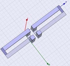 Figure 10. A TSV coupling model that includes the transmission lines
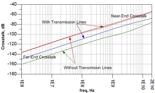 Figure 11. Comparison of crosstalk between TSVs with and without the inclusion of transmission lines
Figure 11 shows that, according to the full wave simulations, there is no measurable difference between the near-end crosstalk as a result of the discontinuity between the transmission lines and the 3D Vias. The difference between the two simulations is very small over the entire frequency range. However, the discontinuity between the transmission lines and 3D Vias will increase the far-end crosstalk. On the other hand, the far-end crosstalk is more minimal than the near-end crosstalk, less significant and never exceeds -50 dB as shown in the simulation.
4. 3D Embedded Crosstalk Test Applications
4.1. 3D Testing Circuit for Crosstalk Induced-Delay and Glitches
In this embedded test application, the coupling effects between adjacent TSVs such as induced-delay and glitches can be investigated for different crosstalk modes. As shown in Figure 12, high speed signals can be fired through three adjacent TSVs at each tier using a multi-edge delay generator circuit. A Mux and Tristate circuits are used to control which signals are active from which tier. The complementary signals are also generated from the delay generator to cover different crosstalk modes. In order to study the effect of phase shifting the aggressor signal on crosstalk induced-delay cancellation, the multi-edge delay generator is used to fine control the delay between adjacent signals.
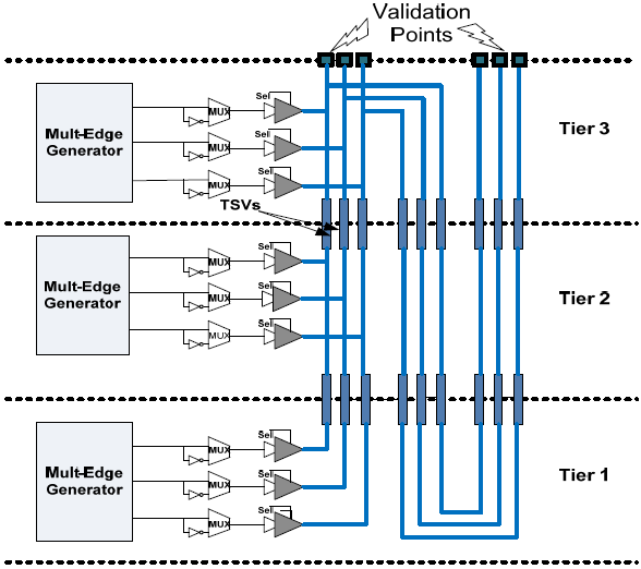 Figure 12. 3D Interconnect crosstalk induced-delay test
Figure 13 shows different crosstalk modes for studying crosstalk coupling on the victim edge. For example; -2X presents the case when both aggressors transition in the same direction as victim. -1X: when one aggressor transitions in same direction and other is quiet. 0X: when both aggressors are quiet or transition in opposite directions or the victim is quiet. +1X: when one aggressor transitions in opposite direction and other is quiet. +2X: when both aggressors transition in opposite direction as victim.
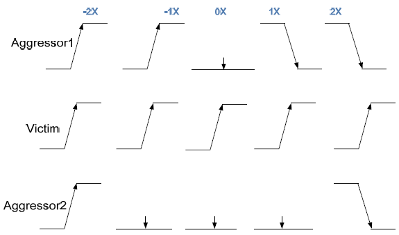 Figure 13. Different Crosstalk Patterns
Figure 14 shows simulated results for the induced-delay crosstalk with different patterns using ADS and 0.25 μm CMOS standard process. The middle graph is the victim line signal with no activity on both aggressor lines. The furthest right and left graphs are -2X and 2X cases respectively, which cause the worst case induced-delay effect. This induced-delay can be mitigated by phase shifting the aggressor signals using the multi-edge delay generator. Figure 15 shows an example of the crosstalk induced-delay cancellation effect after phase shifting the aggressor line 0.8ns for the case of +1X. As graphed, the induced delay due to crosstalk is almost cancelled and the signal aligns again with the 0X case (i.e. without crosstalk).
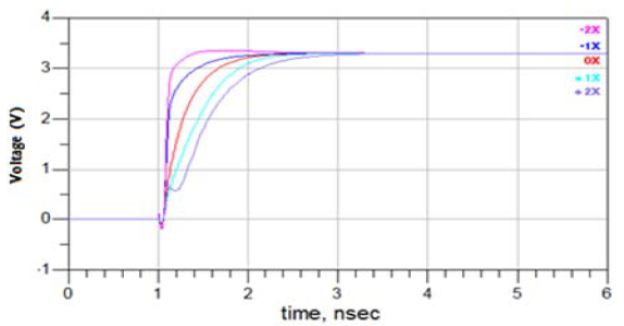 Figure 14. 3D interconnect induced-delay crosstalk for different crosstalk patterns
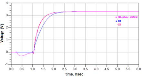 Figure 15. 3D interconnect induced-delay crosstalk cancellation
4.2. Ring Oscillators 3D Crosstalk Test
In this test, a consecutive triggered parallel Ring Oscillators (ROs) structure running same frequency is used to characterize the crosstalk effect between TSVs. Figure 16 shows four triggered oscillators; two oscillators are crosstalk-coupled and the other two are crosstalk-free. The proposed ROs parallel structure creates a delta phase shift difference between each consecutive triggered oscillators, which is equal to the time difference between the delay buffer chain and the oscillation time period of the triggered oscillators. 3D crosstalk detection can be achieved by observing the frequency of crosstalk-coupled oscillators, which is different from the frequency of the crosstalk-free oscillators.
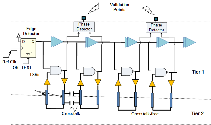 Figure 16: 3D Crosstalk Detection Scheme
Figure 17 shows the output frequency for both crosstalk-coupled (725 MHz) and crosstalk-free oscillators (667MHz).
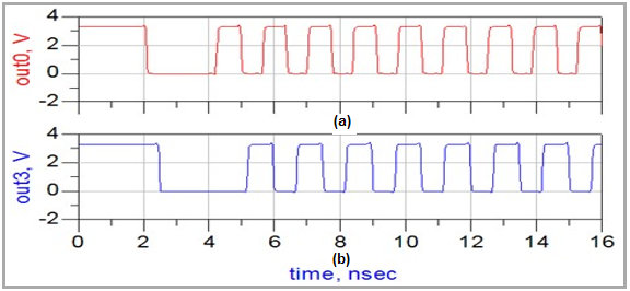 Figure 17: Output frequency for (a) Crosstalk-coupled and (b) Crosstalk-free oscillators
Interestingly, the two crosstalk-coupled triggered oscillators have less oscillation time delay (i.e. faster frequency) than the crosstalk-free oscillators, and the phase difference between the two crosstalk-coupled oscillators diminishes due to the coupling effect as shown in Figure 18. Phase detection at the output of the crosstalk-coupled triggered oscillators can be used as an indicator for strong coupling between TSVs. On the other hand, the edges of crosstalk-free oscillators are still separated by a deterministic phase shift dictated by the time difference between the delay buffer chain and the ring oscillation time period.
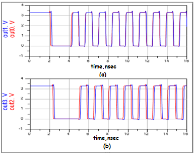 Figure 18: Simulated Results for 3D Interconnect Crosstalk (a) Crosstalk-coupled (b) Crosstalk free
5. Conclusion
In this paper, we presented the signal integrity effects of crosstalk in 3D stacked ICs. A detailed study of TSVs electrical modeling and characterization using HFSS and ADS simulators for frequency and time domains analysis respectively was presented. Simulation results were conducted based on 0.15µm 3DFDSOI process technology from MIT Lincoln lab which present the influence of 3D Vias distances, locations and their structural configurations on crosstalk. The study shows that increasing and decreasing distance of 3D Via signals and grounds respectively can mitigate significantly the effect of 3D crosstalk. In addition, adding more reference Vias and creating a well-defined return current paths have the most impact on mitigating crosstalk. Furthermore, it was shown that the discontinuity between 3D Via and transmission line has negligible impact on near-end crosstalk (NEXT), however; far-end crosstalk (FEXT) might increase but with less significant impact.
Furthermore, a 3D testing circuit application based on a multi-edge signal generator placed at different 3D stacked tiers was studied to evaluate the effect of crosstalk induced-delay and glitches. Additionally, a cross-coupled parallel ROs structure was also presented to evaluate the crosstalk coupling strength effect compared to ROs structure with crosstalk-free TSVs.
- W. Topol, D. C. L. Tulipe, J. L. Shi, D. J. Frank, K. Bernstein, S. E. Steen, A. Kumar, G. U. Singco, A. M. Young, K. W. Guarini and M. Ieong, ”Three-dimensional integrated circuits,” IBM Journal of Res. and Dev, vol. 50(4-5), pp. 491–506, 2006.
- -Q. Lu, “3-D hyperintegration and packaging technologies for micronano systems,” Proc. IEEE, vol. 97, no. 1, pp. 18–30, Jan. 2009.
- R. Davis, J. Wilson, S. Mick, J. Xu, H. Hua, C. Mineo, A. M. Sule, M. Steer, and P. D. Franzon, “Demystifying 3D ICs: the pros and cons of going vertical,” IEEE Design & Test of Computers, vol. 22(6), pp.498–510, 2005
- Q. Lu, “3-D Hyperintegration and Packaging Technologies for Micro-Nano Systems,” in Proc. of IEEE, vol. 97(1), 2009, pp. 18-30
- Tu, “Reliability challenges in 3D IC packaging technology,” Microelectronics Reliability, vol. 51, pp. 517–523, 2011.
- Song, C. Liu, D. H. Kim, S. K. Lim, J. Cho, J. Kim, J. S. Pak, S. Ahn, J. Kim, and K. Yoon, “Analysis of TSV-to-TSV coupling with high-impedance termination in 3D ICs,” in International Symposium on Quality Electronic Design, 2011.
- Tanskanen, J. Toikka, and E. O. Ristolainen, “Crosstalk of wiring in very small 3D module: IMAPS,” 36th International Symposium of Microelectronics, pp. 251-255, 2003.
- Kang; Z. Yan; W. Zhang; J. Wang, “Research on crosstalk issue of through silicon via for 3D integration”, 28th IEEE International Systemon-Chip Conference (SOCC), 2015.
- M. Mak, “Test challenges for 3D circuits,” 12th IEEE International OnLine Testing Symposium (IOLTS), pp. 79–79, 2006.
- Shadi MS. Harb, William Eisenstadt, “A Study of Characterizing Crosstalk Effects in 3-D Vias,” Accepted at the IEEE Latin American Symposium on
Circuits and Systems Conference (LASCAS 2017), Bariloche,, Argentina, Feb 20, 2017 - MITLL Low-Power FDSOI CMOS Process Design Guide, MIT Lincoln Laboratory, 2008.
- Pedram S N M, “Crosstalk-affected delay analysis in nanometer technologies”, International Journal of Electronics, Sept
- Gope D and Walker D M H, IEEE 30th International Conference on. IEEE,“Maximizing crosstalk-induced slowdown during path delay test”, 159-166 , 2012.