Structure-Preserving Modeling of Safety-Critical Combinational Circuits

Adv. Sci. Technol. Eng. Syst. J. 3(1), 472–482 (2018);
 DOI: 10.25046/aj030158
In this work, a representative combinational circuit is visualized in various ways. It is abstracted (concretized) from transistor level to gate level and a structure-preserving transition is carried out into a signal flow graph. For creating a signal flow plan it is necessary to swap the nodes and the edges in the signal flow graph. After having executed this action the result is a signal flow plan. A value table exhibits the coding of the whole circuit. Then the so called module view is used to get the familiar compact and directed display and neighborhood relations are repeated once more, the resolution method is used. It is observed that undefined results can occur in digital circuits. But, these must be avoided in safety critical circuits. These events have to be secured in practice by costly and expensive verification and testing. In order to deal with the problem now, the structure-preserving modeling has to be understood, since this is the only way to achieve a onepurpose, qualitative and cost effective search for errors.
Introduction
This paper is an extension of work orginally presented at the 20th IEEE International Symposium on DDECS 2017, Dresden, Germany [1].
In order to ensure the functional safety of circuits or systems which are regarded as critical to safety, the mutual convert of models and functions is of great importance. The inconsistency problem is omnipresent; therefore, the essential claim for conformity with the formal derived function and the function derived from the real structure has a present role [2]. The directed mode of operation of a system should be represented by a circuit or switching table, also called a table of values, one-to-one in the sense that the encoding can be reproduced. In safety-critical circuits it is necessary not defined results, which often occur in complex circuits, to avoid or to monitor. The transferability of circuits into additional and other display possibilities is therefore a necessary property to ensure the functional safety of safety-critical circuits. In this work, a representative combinational circuit is visualized in various ways. In all these representations, however, it should be noted that the “structure-preserving modeling and transfer” is maintained. This means that the formally derived function must consistently match the function derived from the respective representation type. Both functions must in no case have inconsistencies, since only the fault-free function is included in the circuit. Functional safety can be guaranteed by the condition of the structure-based modeling and transfer. To present the application we use an electrical circuit as a use case. And visualize it in various ways like Gate Level (GL), Signal Flow Graph (SFG), Signal Flow Plan (SFP), Module View (MV), Resolution Method (RM) and KV diagram. During creation of different display possibilities, we explain the rules of the structure-based modeling and transfer. In addition, the mathematical axioms, which are based on Propositional Logic (AA), are declared. The advantage of the method is that each type of representation (respectively presentation) has a depth of accuracy, clarity and compactness. The transferability of circuits into other possibilities of directed representation is a necessary property to ensure the functional safety of safety critical circuits.
Organization of the paper: First, the theoretical foundations are briefly explained in Chapter 2. They are regarded as basic knowledge in order to understand this work. Subsequently, the implementation is described in detail by an example in Chapter 3 and visualized by sketches and models. In the end, the results and the core outline of the work are summarized again and an outlook is given.
2 Theoretical Foundations
2.1 Category level (CL)
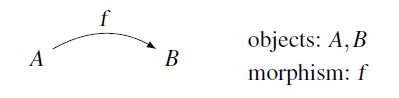 Figure 1: Morphism f from A to B
Morphisms are concretized on category level. A morphism is a directed association between two objects being associative and identitive. In Fig. 1, the morphism f acts on object A and is substituted (=) by object B.
2.2 Value table (VT)
The table of values, also known as truth table or switching sequence table, is a tabular list of the truth value course of a logical statement. In this table, the assignments of the inputs are linked together and the states at the outputs are shown binary. Value Tables (VT) are used for logic operations such as AND, OR, NAND and NOR gates, but also for flip-flops or complex circuits [3], [4]. A value table thus serves to represent the value of a composite statement as a function of the truth values of its partial statements. Tab. 1 shows a truth table for a NOT (left), AND2 (middle) and OR2 (right) function. The input for a NOT function is A and for AND2 and NOR2 the inputs are A and B.
2.3 Combinational circuits (CC)
Table 1: Value table for NOT (left), AND2 (middle) and OR2 (right) function in (0,1)
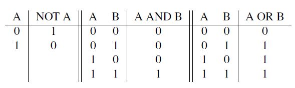
Table 2: Value table for NOR2 circuit
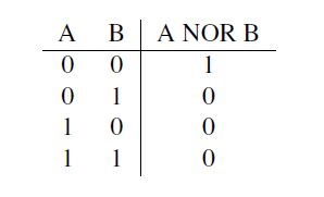
Under a combinational circuit is a circuit that is realized with simple basic gates such as AND, OR and inverters to understand. It realizes a one-to-one mapping, a function. The outputs of this logic are dependent on the inputs, which means there is no feedback from the outputs to the inputs. The output variable is thus only a function of the input variables [4]. Tab. 2 shows the value table for NOR2 circuit. NOR2 represents a combinational circuit, because the circuit does not include feedback.
2.3.1 Abstraction of a circuit
Under an abstraction of a circuit is a kind of “simplified” representation to understand. A complex, combinational circuit is shown in a different way, in order to make it easier to understand. However, in the various representations, the core message of the output circuit must not be changed. So the function of the circuit must not be changed when transferring it to another representation. The circuit must deliver the same function, no matter in which visual presentation it is shown. For example, an abstraction of a circuit is the transfer of a circuit from the transistor level to the gate level. In addition, a circuit can be presented in its module view (MV) (see section 2.10), which is an isomorphism to the signal flow plan of the circuit. The aim of an abstraction of a circuit is the simplified or clearer visual design or presentation.
2.3.2 Structural changeover and modeling
In order to be able to carry out a structure-faithful modeling, it is to be known that two parallel connected transistors are combined in propositional logic as follows. Fig. 2 shows two transistors connected in parallel. VDD is the operating voltage.
It is a complex gate with two inputs (A,B) and one output (C) between which the logical link “OR”exists. This OR2 outputs “1”at the output when one of the inputs are assigned a “0”. This means that if one of the two inputs is assigned a “0”, the output creates a “1”. The two transistors are connected in parallel, they must be concatenated (addition in field algebra). Furthermore the operating voltage VDD has to be considered. It runs in series with each of the two transistors, it muss be catenated (order, multiplication in field algebra) with two transistors.
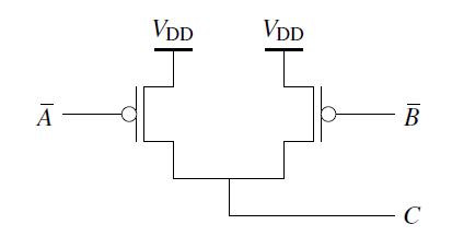 Figure 2: Example of parallel connected transistors
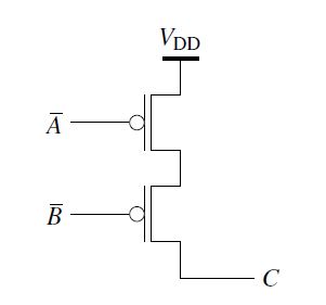
Figure 3: Example of serial connected transistors
If C in Fig. 2 is to be expressed as a function (contrary to logic, only true values can be processed in propositional logic (see section 2.9)), then this is:
C =VDD·(A+B) (1)
In Fig. 3 two transistors are connected in series. It is a complex gate with two inputs (A,B) and one output (C) between which the logical link “AND”exists. This AND2 outputs “1”at the output when both inputs are assigned a “0”. This means that if both of the two inputs is assigned a “0”, the output creates a “1”. Furthermore the operating voltageVDD has to be considered. It runs in series with each of the two transistors, it muss be catenated with two transistors. C can be expressed in propositional logic as follows:
C =VDD·(A·B) (2)
Structure-faithful modeling unites function and structure one-by-one in the sense of a monomorphism injective that is, the structure has at most one solution (this is the function) – and of a epimorphism surjective – that is, the function has at least one solution (that is the structure). Such a mapping enables a one-to-one (local-bijective) and understandable description of a generating system. During transferring into various presentation possibilities the structure-faithful modeling has a significant role. It is extraordinary important that the formally derived (modeled) function coincide with the function generated by the real structure. Consequently the function has to correspond to reality and shall not exhibit any inconsistencies. Only in this way the functionality of a circuit can be ensured. Structure-faithful therefore means that the relation to reality must never be lost during modeling. Shortly spoken, each pin of the model at gate level (GL) must show up in the real world at transistor level (TL). But, pins have to be correctly labelled in reality at transistor level (TL). This is mandatory.
During the transfer, it is also important that the function generated from the real structure consistently matches the function derived from the signal flow graph or any other type of presentation. Only in this way the functionality of the generating circuit can be ensured. In addition, there is a structure-based transfer only in the absence of inconsistencies. A transfer of the signal flow graph or of the circuit into a value table must also be structure-faithful. Thus the function derived from the evaluation table must correspond to the same function derived from the signal flow graph or the generated circuit. Shortly spoken, each undefined pin of a given reality or not proper assigned signal of a given model has to be shifted to undefined. We consistently use the symbol “∗”.
2.4 RS Buffer
In complex circuits, many structures exist that can create undefined results. These undefined results must not occur in safety-critical circuits, since otherwise the desired function of the circuit cannot be guaranteed. For this reason, the RS buffer structure is established [2]. It can intercept undefined cases in combination with a dual-rail approach.
Thus, it is possible to stabilize a complex circuit in its function without glitch. These stabilized states do not produce unpredictable events and can therefore be processed by the circuit without causing errors. Fig. 4 shows the circuit symbol and Fig. 5 shows the circuitry of the RS buffer. The value at the node X in the circuit corresponds to the value at the pin Y, because of the inverter. Thus, the X is neglected for the sake of clarity in the VT of Tab. 3. On closer examination of Tab. 3, it is noticeable that the RS buffer triggers a switching process only during assignments (S,R)=(1,0) and (S,R)=(0,1). The old state is retained for assignments (S,R)=(1,1) and (S,R)=(0,0). The function for the output Y is therefore Y = R(S∨Y)∨S(R∨Y)=YR∨YS∨SR.
Table 3: Value table of the RS buffer [2]
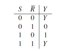
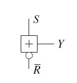 Figure 4: Circuit symbol of the RS buffer
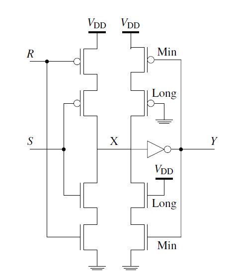
Figure 5: Circuit of the RS buffer [2]
2.5 Signal flow graph (SFG)
The signal flow graph (SFG) is a vividly method to present the internal structure of a system or the interaction of several systems. This presentation allows a better understanding of the function as well as the interrelations of one or more systems. In addition, the signal flow graph is the appropriate tool for abstracting functions or connections to one level above category level (associativity and not identity). The signal flow graph is a directed and weighted graph whose nodes represent objects (sets) and its edges morphisms (functions). The edges of this graph can be understood in a dual view (SFP) as small processing units which process incoming signals (edges) in a particular form and then send the result to all outgoing edges (signals). Signal flow graphs are formally defined graphs [5]-[9].
2.6 Signal flow plan (SFP)
The signal flow plan (SFP) has a special significance in control engineering and, with the representation method, is based on a block diagram and adds to a further loan of the relationships within a system. A signal flow plan is used to identify the complexity of a system. This contains unidirectional blocks, also called nodes, which transmit incoming signals as small processing units into outgoing signals. In the signal flow graph these are represented by edges. From an SFP, the transfer function of a system can be derived. The signals are redirected to edges, unlike the signal flow graph. In the signal flow graph, they are represented by nodes. Edges in a signal flow plan are also directed connections between two nodes. They illustrate the effect of a signal by its weighting. Furthermore, it is possible to transfer a signal flow graph into a signal flow plan by transferring nodes into edges and edges into nodes [5], [7], [9]. Fig. 6 shows a simple example of a signal flow plan derived from a signal flow graph. The input signals x0 and x1 adds up to an output signal y.
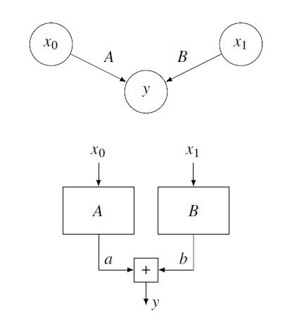 Figure 6: From a signal flow graph (above) to a signal flow plan (below)
2.7 Boolean algebra (BA)
The switching algebra (boolean algebra) is based on decisions and comparisons, so it can explain and visualize logical links very well. Successful results are represented by a “1”, unsuccessful results by a “0”. These two symbols are complementary to one another. At any time, each pin must be occupied, because only then the system can be a total system and can be calculated by the switching algebra. The switching algebra is not sufficient for a detailed representation of a circuit. However, it is suitable for the functional description without restrictions to the general [10].
2.8 Positive logic (PL)
In the positive logic the symbol “1” stands for a successful event. Unsuccessful events are called undefined. Positive logic is an event that occurs just as it is expected. This means that if a negative event is expected and it occurs, this event is considered successful. This also applies analogously to a positively expected event. If a positive event is expected and it occurs, then this event is also successful. In the positive logic, therefore, only the “1” exists as a value [11]. Here, we need a “0”, too. Therefore, the “0” is also a “1” but only a part (child) of the “1”.
2.9 Propositional logic (AA)
The propositional logic comes from the formal logic and can be continued into the switching algebra without restrictions to the general. This “Aussagenlogischer Ausdruck (AA)” describes the relationship between statements. Statements can be seen partially in the propositional logic. This means that there should be only one unary statement. The symbols are true (w) and not false (f). The following example is intended to illustrate the propositional logic: The statement Y = (A∧B)∨C contains two statements and is nevertheless unary, regardless whether is equal to a positive literal or a negative literal. The following statement contains only one statement and is also unary Y =(A∧B). Thus, in AA a statement is always true, only its complemented content can be interpreted as “false”. The logical sign for a true statement is “w ” or “f” [11], [12].
2.10 Module view (MV)
Through a model representation, a real system can be displayed simpler and clearer. The natural section of reality can be simplified by model visualization, and the model representation can also serve as a reference model for further development of a system. In order to represent a real circuit with real electrical components as a model, the structure-faithful transfer is of great importance. In addition, it is necessary that in safety-critical circuits, the modeling is performed structurally, because only then the structure-related functional safety of the circuit is guaranteed. This means that the formally derived and modeled function with which the function created by the real structure must be absolutely identical. Fig. 7 shows a simple example of the asymmetric and irreflexive module view. Due to the directed representation as a module view, a clear visualization is achieved. You can see the input (input vector) X, the output F and the programming vectors Z and Y. By presenting it as a module view, the complexity of the representation can be completely directed.
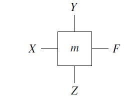 Figure 7: Example of a module view
Only the inputs, outputs and programming vectors are seen. The function, how exactly the interaction of these variables ever is, is not described and explained. The function (transitive closure) is represented by m (model) [5].
2.11 Resolution method (RM)
The resolution method (RM) is a method to check the truth value. It is primarily about being able to prove the satisfiability or unfulfillability. In order to provide this proof, a clause set is extended by new clauses, called resolvents, until an empty clause is generated. If this succeeds, the initial quantity is unsatisfiable. Here, the clauses are conjunctions. A set of clauses, therefore, is a disjunction. It follows that if an empty clause can generated, the initial set is tautological. Resolvent of clauses C1 and C2 (according to literal l) is given in [13]. An example of the resolution method is shown in Fig. 8. Here you can see that the clause set can be non-tautologically fulfilled, since in the end no empty clause can be generated. Will be a clause set with the resolvent resulting from their clauses, this results in a logically equivalent set of clauses. This can be reunited with its resolvents without affecting satisfiability, and so on. If finally the empty clause can be formed, a tautological set is proven. In the other case, for example if the last clause is not empty, this is the proof of the satisfiability of the disjunvtive clauses.
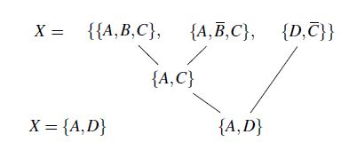 Figure 8: Example of a resolution
The resolution method obeys the following neighborhood relations:
- The resolver {y,z} (largest common cover) can be generated from the clauses {x,y} and {x,y,z}.
- The resolver {} can be generated from the clauses {x} and {x}.
Definition: Let C1 be a clause containing the literal l and
let C2 be a clause containing the literal l. Then the clause is called:
C =(C1\{l})∪(C2\{l¯}) (3)
2.12 KV diagram
The Karnaugh-Veitch diagram (KV diagram) is used for the clear presentation and simplification of Boolean functions into a minimal expression. A KV diagram can be used to transform any disjunctive normal form (DNF) into a minimal disjunctive logical expression. The diagram is labeled with the variables at the edges. Each variable occurs in negated form (negative literal) and not negated form (positive literal). The assignment is arbitrary. However, it should be noted that horizontally and vertically adjacent fields may only differ in exactly one variable [4].
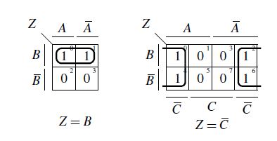 Figure 9: KV diagram examples
Minterm Method:
- Try to group as many horizontally and vertically adjacent fields as possible that contain a “1” (1, 2, 4, 8, 16, 32, …).
- A block may continue over the right / left or bottom of the chart.
- From these identified blocks so many are to be selected that all “1” fields are covered (Fig. 9).
- Now the conjunct terms are formed.
- These conjunctive terms are linked with an OR and a DNF results.
Maxterm method: This method differs from the Minterm method in the following points:
- Instead of ones, zeros are combined into blocks.
- Subsequently, disjunction terms are formed.
- These disjunction terms are AND, resulting in a conjunctive normal form (CNF).
3 Implementation
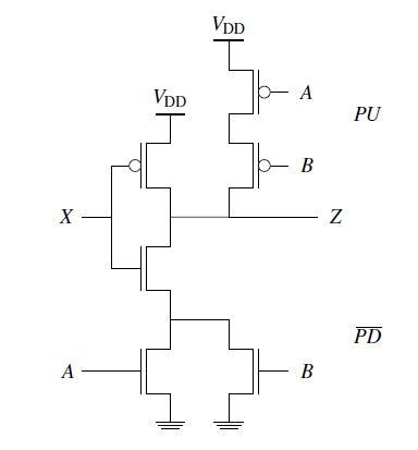 Figure 10: Simple electrical circuit at transistor level (TL)
In this Chapter, an electrical circuit is considered at the transistor level in Fig. 10. Afterwards, the circuit is transfered from the transistor level into the gate level in a structured manner. It should be noted that the analog circuit, that is, the circuit at transistor level, is described at the gate level in propositional logic. Subsequently, the circuit is converted into a signal flow graph and signal flow plan at the gate level. Various possibilities for the representation of the output circuit, then such as the evaluation table, the module view or the resolves are presented. With all these possibilities of representation, it should be noted that the respective derived function must not have any inconsistencies that means, the formally derived function must agree with a function generated from a real structure (TL). Fig. 10 shows the circuit at the transistor level, this circuitry is a combinational circuit because there are no feedback lines, which is to be transferred to the gate level. It is a complex gate with three inputs and an output.
3.1 Concretization to gate level
The analysis of a circuit at the transistor level is more detailed and more complex than viewing at the gate level, since the representation in gates is only a “model”which allows a simplified and clear view of the circuitry. The transfer of a structure at the transistor level into a structure at the gate level is therefore a concretization (often called abstraction) and serves to increase the clarity and simplify the understanding of the structure. From propositional logic and category point of view, however, transistor level (parent) is the abstraction of the gate level (child). This is important to keep in mind.
In the first step is now the electrical circuit transferred to the gate level. First, the pull-up (PU) and the pull-down (PD) are viewed separately from each other. When the transistors of the pull-up or pull-down are connected in parallel, they must be concatenated. On the other hand, when the transistors are connected in series, they must be catenated. Furthermore the operating voltageVDD has to be considered in the pull-up. This runs in series with each of the two lines of the pull-up. And the mass potential runs serially to both line of the pull-down.
The transistors in the PU are switched with a “0” low-active input and the transistors in the PD are switched with a “1” high-active input. PU and PD are connected by a composition (concatenation). With the composition it is meant that different things are substituted but do preserve their directed manner (the morphisms are preserved). This composition ensures the RS buffer in Fig. 5. In Fig. 5 after the pulldown, a switch “¬”is installed in order to meet the propositional composition (we use switch to replace the two levels “0” and “1”, we can switch from one level to another). The function of the RS buffer has already been explained in the basic chapter. The operating voltage is usually designated withVDD, the reference point is the mass with the low-active input GND (since the gate level has been in AA, the ground is written as GND). Please keep in mind that pins have to be coded correctly. You have to choose the correct literals, either positive literals or negative literals.
In the second step subcircuits are described as concrete mathematical functions in the propositional domain (in the AA domain). It should also be noted that each partial circuit is basically at least disjunct, in this case even complementary, this mean a pull-up (PU) and a pull-down (PD). Pull-up means that the output is pulled up to the operating voltage VDD. This part of the circuit is low-active since a logical “0”must be present at the primary input in order to trigger the switching process. The PD draws the output to the mass potential. It is referred to as high-active, since a logical “1” must be present at the primary input, so that a switching process is triggered. For example, Tab. 3 shows the functionality of the RS buffer. The operation is assumed to be already known. Thus, the circuit consisting of a PU and a PD has the following equation:
Y = PU +¬PD = S+¬R (4)
Eq. 4 will play an important role in the later course of the work. After all steps, as explained above, have been carried out, a structure-preserving model at the gate level results. Important is, that during all steps inconsistencies must not occur. In Fig. 11, the electrical circuit is now displayed in propositional logic at gate level. As described above, the PU and PD are summarized using the composition. In addition, a switch is built between PD and the composition. Its task is also to highlight the low-active input of the RS buffer. It is important that the stars here in the continuation only serve as a “monitor”for checking. If the circuit is designed correctly, each star (∗) can only supply a “0”.
In the third step, the node Z (pin Z) is expressed in a function: The PU and PD is connected to the composition “+”. The operating voltage VDD flows in series with the inputs in the PU. The mass runs serially to all inputs in the PD. The switch between composition and pull-down switches the logic value of the last part to a negative literal – the substitute of its complement in Eq. 4. In summary, it should be emphasized that viewing at the gate level (in propositional logic) allows a directed and more simplified view, which makes the derivation of the function at node Z easier. The node X is treated as another input. Thus, it must be noted that node X affects the PU and the PD. Furthermore, the PU and the PD are linked by a composition. This composition works like an RS buffer. The inputs are then linked to the logical operators. Not to forget is the switch, which is between PD and the composition. This “switches” the part of the function belonging to the PD. The operating voltage VDD and the mass run serial to the inputs. The stars (∗) also serve (Fig. 11) for to check the correctness of the circuit. For example, each individual star can only assume the value “0” in order to ensure that the circuit is correctness. Fig. 11 shows the structure-faithful modeling of the circuit at gate level (in AA). After the circuit is transferred to gate level, the node Z can be expressed as a mathematical function in Eq. 5.
Z =VDD·(X +A·B)+¬(GND·(A+B)·X) (5)
The circuit at gate level in Fig. 11 shows the concreteness of the output circuit (Fig. 10). As described above, it was transferred from the transistor level to the gate level in a structure-preserving manner. The functions derived at the transistor level and the functions derived at the gate level must be identical with respect to their partial order (directed manner), this means the function of the circuit must not be changed by the transfer. Only then is the transfer a structure-faithful one.
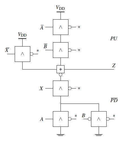 Figure 11: Simple electrical circuit at gate level (in AA)
The gate level can be viewed as a model view. It serves to increase clarity as well as contribute to an understanding of the circuit.
3.2 Transfer to a signal flow graph (SFG)
With the basic knowledge from Chapter 2, the function Z is now transferred step by step into an SFG at Fig. 12.
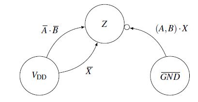 Figure 12: SFG of electrical circuit
For the creation of SFG, it is determined which signals are visualized in a node and which are represented by an edge. The operating voltage VDD and the ground GND are visualized by a node, while the inputs, also the X, are used as edge weights for the processing of the signals. The operating voltage is catenated by the inputs A, B and X. Please remember that we are in propositional logic. The negative literal A is not the complement of A but can be substituted by the complement of A, A = A. BA is constituted by A = ¬A. Thus, VDD represents a node while the inputs with the switch reside on the edges. The third edge has as an edge weight the catenation of the X with the two inputs A and B. The mass is represented as a node. The switch (bubble at node Z) must be considered as shown in Fig. 12.
These three edges end at to the node Z. The switch, which must be installed here, is not to be forgotten. These two edges concatenate to the node X. When looking at the Z function it is noticeable that the node X has a major influence on this function:
It is important that the function Z generated from the real structure is consistent (in the direction) with the functions derived at the gate level and the signal flow graph. The SFG allows a further comprehensible and simple visual consideration of the problem. The system is represented simply and visually by weighted, directed graphs. In dual sense (SFP), blocks are small processing units that process incoming signals (that are edges) in a certain form and send the result to all outgoing edges (that are signals). In Fig. 12, the comma “,” means in parallel. We use the comma “,” to write different things next to each other but preserving the directed manner. Since the directions have to be preserved in the structure faithful modeling and transfer, we announce two edges A and B next to each other. From Fig. 12 follows equation 6:
Z =VDD·(X +A·B)+¬(GND·(A+B)·X) (6)
3.3 Transfer to a signal flow plan (SFP)
As already explained, the node can be interpreted in the dual sense as a partition, a signal, and an edge over its weight as processing (operation) of the signal. Thus it generates (substitutes) a new signal. The states of the output circuit are to be found in the nodes. The edges are supplemented with their weights. If the electrical circuit is now considered more closely at gate level, the background knowledge of this work can be used to derive a signal flow plan. It is important to know that the function which is derived from the signal flow graph has to coincide with the function which is derived at the gate level. For only then the modeling has been done in a structured way and the relation to reality has not been lost. In order to be able to transmit a signal flow graph into a signal flow plan, the following must be carried out. By interchanging nodes and edges, a signal flow graph results in a signal flow plan and vice versa.
In order to set up a signal flow plan one has to determine which signals are visualized in a node and which are represented by an edge. The edge is a directed line, which connects two nodes and effects the processing of a signal via its weight. The mass as well as the operating voltage represent the nodes in the SFG. The primary inputs are shown as edges. The signal flow plan (action plan) is used to determine the complexity of a system. The nodes (blocks) in a signal flow plan are small processing units that transmit incoming signals on edges into outgoing signals on edges.
Fig. 13 shows the signal flow plan derived from the signal flow graph of the electrical circuit. The signals, in this case the edges (nets) of the signal flow plan, are found on the nodes of the signal flow graph. The nodes (blocks) of the signal flow plan are found in the edges of the signal flow graph. After the gate level of node Z has been transferred to a signal flow plan, the signal flow plan is displayed in a module view (Fig. 14).
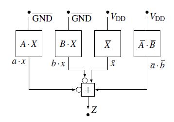 Figure 13: SFP of an electrical circuit GND
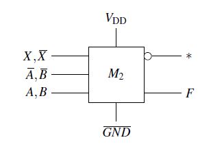 Figure 14: Module-view of an electrical circuit
This digital structural element serves for further simplified viewing of the real system. This further simplifies the understanding of the structure. The module-view for node Z has:
- an input vector (inputs): A, B, A, B and X,X
- a programming vector (states): GND and VDD
- an output vector (output): Z =: F
As the MV is using the transitive closure it preserves all pins (that occur in reality). Therefore, it is structure-faithful and a compact presentation of the circuit. Within M2, the function is outdated here. We can convert this function from MV to other display posibilities structure-faithful. At the star (∗) we should only observe the “0”.
3.4 Evaluation table of the circuit
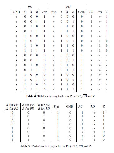
In the next step the node Z (Eq. 7) of the output circuit (Fig. 11) is shown in the form of a total switching table (in positive logic (Tab. 4), followed by the partial switching table in positive logic (Tab. 5).
Z =VDD·(X +A·B)+¬(GND·(A+B)·X) (7)
The function in Eq. 7 can be expressed as follows:
Z =(Z,Z)=VDD·(X +A·B),¬(GND·(A+B)·X)=VDD·(X +A·B)+¬(GND·(A+B)·X)= PU +¬PD (8)
In Eq. 7, node Z is represented in different versions. Z = (Z,Z) means that Z is a partition of two blocks provided by a positive and a negative literal. The last part of Eq. 7 means that Z consists of two parts, the pull-up and the pull-down. The relationship between PU and PD is the same as already shown in Eq. 4, not to forget the composition “+” between PU and PD, the RS buffer.
Tab. 3 is also required in order to be able to set up the switching table. The operating voltage VDD depends on the pull-up. It is important to know that if only the operating voltage supplies a “1”, a reliable switching process can be present in the PU. The pull-down depends on the mass, GND. A switching operation in the PD can only take place when the mass is at “0”.
Tab. 4 shows the total switching table of node Z in positive logic (PL). On closer examination of the table it can be seen that this table is composed of three divisional tables. The result of the PU and the PD and the node Z represent a further table. The coding universe for the PU consists of the operating voltage VDD and (A,B,X). For the PD, the coding universe consists of (A,B,X) and GND. Thus the table for the PU and PD has a total of 24 = 16 assignments. The output Z represents the respective state for the one-to-one coding of the table.
The lower part of the table (last eight lines) represents assignments which tend not to trigger any switching operations. The reason for this is that during the pull-up the operating voltage VDD can only assume the value “1”. The mass does not matter. For pull-down, GND must only have the value “0”, so that a switching operation is triggered. The operating voltage does not matter.
The results of the pull-up and the pull-down are calculated by Eq. 7. In order to determine the resulting node Z, Tab. 3 is to be considered. It represents the relationship between PU and PD. In the next step, the total switching table Tab. 4 (in PL) is transferred to a partial switching table Tab. 5 (in PL). The correctness of the partial switching table is only given because a structure correct transformation and modeling has taken place. This ensures that the circuit has been designed without errors and thus a partial switching table can be applied without errors. Tab. 5 shows the partial switching table of node Z. The operating voltage is unsignificant for the PD, whereas in the PU it can trigger a switching operation only with a “1”. The mass is meaningless for the PU, whereas only a “0” the mass in the PD, triggers a switching process. Thus the last eight lines of the total switching table is lost. For the safety of a defect-free structure it can be firmly assumed that in these assignments, the output Z assumes the states in Tab.5. The symbol ∗ represents undefined.
3.5 Resolution method for the circuit
In the last step, the node Z (Eq. 9) of the output circuit (Fig. 11) is entered into a KV diagram.
Z =VDD·(X +A·B)+¬(GND·(A+B)·X) (9)
For this purpose, Eq. 9 must be converted into a DNF system, as can be seen in the following.
Z =VDD·X +VDD·A·B+¬(GND·A·X)+¬(GND·B·X) (10)
Due to the different terms of the Eq. 10, a better understanding of the KV diagram is to be developed in Fig. 15. It is noticeable that some fields overlap in the diagram. In particular, this fields are occupied by “1” and “¬1”. The question is how this field actually looks in the KV diagram in AA. Now Eq. 10 is a concrete equation (Category Level). The KV diagram for this equation is to be represented in AA. In this case, the switch “¬” is substituted by complement since the KV diagram is in the Aussagenlogik (AA), the propositional logic, the logic of statements. The KV diagram now looks as Fig. 16. The blocks of the KV diagram (Fig. 16) are now determined from Eq. 10 as follows:
(A∧B∧VDD)∨(X ∧A∧GND)∨(B∧X ∧GND)s∨(X ∧VDD)∨(VDD∧GND) (11)
Therefore in Eq. 11, VDD ∧ GND represents a redundant block, a redundant prime implicant. This case is visualized by dashed lines. This part of the equation is now used for resolving. Fig. 17 shows the resolution method for node 1. The clauses ({A,B,VDD}, {X,A,GND}, {X,B,GND},{X,VDD}) are derived from Eq. 10. In order to be able to determine the clauses, the equation was first transformed into a DNF system in order to connect the switch neglected. Only by neglecting the switch can a resolvent be formed. In order to determine the folowing clauses ({A,B,VDD,GND}, {A,B,VDD,GND}, {X,A,GND,VDD},{X,A,GND,VDD}, {X,B,GND,VDD}, {X,B,GND,VDD}, {X,VDD,GND}, {X,VDD,GND}), the ones in the KV diagram (Fig. 16) have to be viewed individually. {VDD,GND} comes from prime implicant (dashed lines) of Fig. 16.
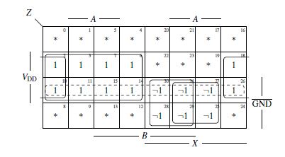 Figure 15: KV diagram for Z (electrical circuit in PL)
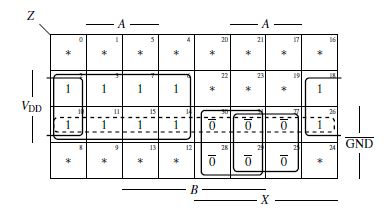 Figure 16: KV diagram for Z (electrical circuit in AA) {VDD,GND}
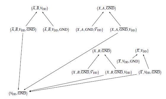 Figure 17: Resolution method for the electrical circuit in PL
So it is noticeable that the KV diagram shows additional information when looking at the ones. The ones that can be useful in resolving are selected. Resolves can be generated only from certain clauses. As already explained in Chapter 2, the following holds: The resolver {y,z} can be generated from the clauses {x,y} and {x,y,z}. The resolver {} can be generated from the clauses {x} and {x}. The prime implicant (dashed) in the KV diagram is made up of this clause:
VDD, GND.
This clause resolves from three different clauses, as shown in Fig. 17.
4 Conclusion
The transferability of circuits into other possibilities of representation is a necessary property to ensure the functional safety of safety critical circuits. In this work an output circuit has been visualized in various display possibilities. Each type of presentation has its advantages and disadvantages. Moreover, each type of representation has a depth of accuracy, clarity and compactness. However, all of these representations are common in that their “structure-faithful modeling and transition” must be preserved. This means that a formally derived function has to match consistently with the function derived from the respective representation type. Both functions must in no case have inconsistencies, because only then the fault-free function of the circuit can be maintained. Shortly spoken, each pin of the model at gate level must show up in the real world at transistor level. But, pins have to be correctly labelled in reality. This is mandatory.
- R. Rasim, C. Kocar, S. M. Sattler: Structure- Preserving Modeling of Safety-Critical Combinational Circuits, 20th IEEE International Symposium on DDECS 2017, Dresden
- Uygur, S. M. Sattler: Structure-Preserving Modeling for Safety Critical Systems. Mixed-Signal Testing Workshop (IMSTW), 2015
- M. Mano, R. K. Charles: Logic and Computer Design Fundamentals, Third Edition. Prentice Hall, 2004
- Horowitz, W. Hill: The Art of Electronics, Second Edition. Cambridge Press, 1989
- C. Dorf, R. H. Bishop, Modern Control Systems Solution Manual, Pearson Studium, 2011
- J. Mason, Feedback Theory – Further Properties of Signal Flow Graphs, IEEE, vol. 44, pp. 920-926, 1956
- S. Levine, The Control Handbook, CRC and IEEE Pres, 1996
- A. Brzozowski, E. J. McCluskey, Signal Flow Graph Techniques for Sequential Circuit State Diagrams. IEEE vol. EC-12, pp. 67-76,1963
- M. Horowitz, Syntehsis of Feedback Systems, Academic Press INC. London, 2013
- S. Stankovic, J. Astola: From Boolean Logic to Switching Circuits and Automata, Springer, 2011
- H. Hackstaff: Systems of Formal Logic, Springer, 2012
- Posthoff, B. Steinbach: Logic Functions and Equations, Springer, 2009
- Leitsch: The Resolution Calculus, Springer, 1997