Morphological and Optoelectrical Characterization of Silicon Nanostructures for Photovoltaic Applications
 , Moussa Toure 2, Modou Beye 1, Diouma Kobor 2, Amadou Seidou Maiga 1
Adv. Sci. Technol. Eng. Syst. J. 4(1), 45–49 (2019);
 DOI: 10.25046/aj040106
Metal (silver)-Assisted Chemical Etching (MACE) method is used to fabricate silicon nanostructures like silicon nanowires (SiNWs) and silicon nanocones (SiNCs). The morphological characterization of fabricated SiNWs has shown that 5 minutes is the optimal time of silver deposition on silicon substrate. Silicon nanocones (SiNCs) were also fabricated by etching vertical SiNWs with a AgNO3=HF=H2O2 solution. The optical and electrical properties of SiNWs and SiNCs are analyzed and compared with those of the bulk silicon. The fabricated SiNWs (SiNCs) reduce the surface reflectance and the sheet resistance down to 6% (3%) and 9.143 /sq (6.997 /sq) respectively.
1. Introduction
The energy demand worldwide is largely greater than the energy supply. Thus, the conventional energy sources (oil, coal and nuclear) become expensive. In the other way, these conventional energies have nega- tive impact on the environment and the human health. The explosions of the Chernobyl and Fukushima nu- clear power stations cause damage on the human health in many countries [1][2]. Consequently, the development of alternative energy sources is urgently needed. Solar energy, as a clean, abundant and renew- able source, is one of the most promising alternatives to conventional energies.
The incident light is converted into electric current by photovoltaic (PV) cells. The PV cells are fabricated by using semiconductor materials. Among the semi- conductor used in the PV cell fabrication, the bulk silicon (mono or multi-crystalline) is mostly domi- nated. The best conversion efficiencies obtained with monocrystalline (multi-crystalline) silicon solar cells and modules are around 26.7% (21.9%) and 24.4% (19.9%) respectively [3]. However, the crystalline sili- con represent about 40% of the production cost of bulk silicon modules [4].
Further cost reduction and efficiency enhancement, through reduction of material usage, simplification is to use silicon nanostructures, which theoretically should be both more efficient and less expensive [5].
The common methods to fabricate silicon nanos- tructures (SiNWs, SiNCs) are dry etching and lithog- raphy methods [3][6]. However, these methods are complex, expensive, and unsuitable for mass produc- tion. One of the alternative methods is to use Metal Assisted Chemical Etching (MACE) which is based on the strong catalytic activity of metals in HF/H2O2 aqueous solution [7]. This low cost method is very easy to implement and it allows to realize various silicon nanostructures with excellent optoelectronic proper- ties without changing the purity of silicon.
Dimova Malinovska et al. [8] are the first to etch the silicon by using MACE method. They demon- strated that porous silicon can be obtained by using aluminum metal and HF/HNO3/H2O solution. Since 2002, the MACE method is being improved and a va- riety of nanostructures are fabricated. SiNWs were firstly fabricated by Peng et al. They used the mixture of HF/AgNO3 [9][10]. Vertical SiNWs were fabricated by combining MACE and lithography methods [11]. However, the cost of these nanowires is relatively high because of the lithography technique used to deposit the PS sphere masks. Moreover, Au metal was used as catalyst. To realize best silicon nanostructures without using any mask patterns and expensive metals is required in the solar cell manufacturing.
The objective of this work is to fabricate silicon nanostructures (nanowires and nanocones) by MACE method in ambient temperature, without using any mask patterns, and to study their structural and opto- electronic properties.
2. Materials and method
The silicon nanostructures were fabricated by using (100) p-type monocrystalline silicon substrate. These samples have a resistivity and a thickness in the ranges of 1-5Ω/cm and 600 – 650 µm, respectively.
The different steps of the SiNWs fabrication by
MACE are summarized in the figure 1. First, the samples were cleaned by using, respectively, acetone, ethanol and deionized water in the ultrasonic bath for 15 minutes. After this cleaning, the samples were immersed in a piranha solution (H2SO4/H2O2) for 10 minutes to eliminate any organic trace. The last step of the cleaning process was to use a diluted HF solution to remove the native silicon oxide SiO2 and to rinse the samples with deionized water. After the cleaning steps, the samples were immersed in the HF/AgNO3 (4.8M/0.02M) solution for a chosen time in [0.5, 2.5, 5, 10, 15, 30, 60, 120 minutes]. This solution allows to deposit silver (Ag) nanoparticles on the silicon sur- face. After depositing Ag nanoparticles, samples were
directly immersed in HF/H2O2 (4.8M/1.176.10−3M) mixture. This solution is responsible for the etching
silicon. After the etching process, all Ag waste inte- grated into the silicon substrate must be removed. For this, a diluted HNO3 solution was used.
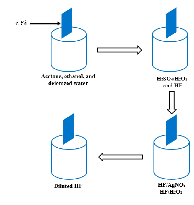 Figure 1: Different steps in the fabrication of the silicon nanowires by MACE
The conical form of silicon nanostructures can be fabricated by MACE via obtained silicon nanowires (SiNWs). For this, SiNWs are introduced into AgNO3/HF/H2O2 solution. This solution have dou- ble functions. First, it deposit Ag nanoparticles on the top of SiNWs. And second, it etch these SiNWs at the top to form truncated SiNWs like silicon nanocones (SiNCs). It is interesting then to understand how these nanos- tructures occur on the surface of silicon substrate.
3. Mechanism of the formation of silicon nanostructures
The growth mechanism of SiNWs is described by Peng et al.[12]. The Ag+ ions given by HF/AgNO3 seize the valence band electrons of silicon. Thus, these ions be- come now Ag nucleation. Ag nuclei gradually grow into Ag nanoparticles. The reduction of H2O2 oxydant is done at Ag nanoparticles; and the holes are con- sumed by the silicon oxidation. The produced silicon oxyde is quickly dissolved by HF. Ag nanoparticles travel into the silicon wafer as the silica layer is dis- solved, thus the depth of Ag nanoparticles in the pit increase gradually with the increase of the reaction time.
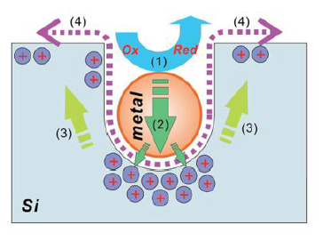 Figure 2: Formation mechanism of silicon nanowires fabrication: (1) reduction of oxidant H2O2, (2) injec- tion of generated holes onto the silicon substrate, (3) migration of holes inside the silicon surfaces, and (4) dissolution of silicon oxide by HF [13]
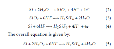
The Ag nanoparticle side in contact with the etch- ing solution acts as a cathode and serves to reduce H2O2 (see the equation 1). The other side of Ag par- ticles which is in contact with the silicon substrate functions as an anode that serves to oxidize silicon which generates H+ and electrons (see equations 2 to 4). A considerable difference of potentials between the cathode and anode sites is then created and therefore a local oxidation current flows from the cathode site to the anode one.
![]()
 The same reactions can explain the formation of silicon nanocones by etching the SiNW tops. Indeed, when the sample is put in AgNO3/HF/H2O2 solution, Ag nanoparticles are deposited on the SiNWs. Thus, H2O2 oxydises the SiNW tops and silicon oxyde is re- duced by HF. These oxydation and dissolution will oc- cur at the same time during the etching process. Then, silicon nanocones will be formed on silicon substrate by truncating the edge top of SiNWs, according to the study of Shimizu et al.[12].
A MERLIN Scanning Electron Microscope (SEM) with Zeiss FEG was used for structural characteriza- tion of the elaborated silicon nanowires. The spectral reflectance of fabricated silicon nanostructures is mea- sured by Hitachi UV-VIS-NIR 4001 spectrophotometer equipped with an integrating sphere. Their electrical properties are studied by measuring the sheet resis- tance with 4-point probes method.
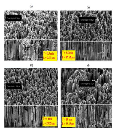 Figure 3: SEM images of silicon nanowires fabricated by the MACE method
4. Results and discussions
Figures 3 and 4 show the SEM characterization results of the fabricated SiNWs. The SiNW height (L) depends on the deposition time of silver nanoparticles (T). The SEM characterization results show that L increases
with T. Therefore continuous film of Ag nanoparticles can be obtained by increasing T. This continuous film with a few holes permits to obtain well-defined SiNWs [13]. However, a spongy structure is shown when T is very high (more than 30 minutes). It can be explained by the break of long SiNWs. Moreover, a structure with too much spaced SiNWs, is obtained for too long deposition time of silver nanoparticles. This spacing of nanowires as function of the etching time could be due to the phenomenon of the coalescence of silver nanoparticles which leads to the etching of the silicon under the silver macroparticles.
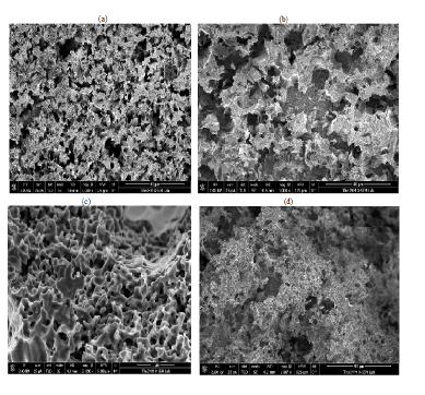 Figure 4: SEM images of silicon nanowires fabricated by MACE method for (a) 15 minutes, (b) 30 minutes, (c) 60 minutes and (d) 120 minutes.
The reflectance of the fabricated SINWs was mea- sured and the results are shown in figure 5. In this figure, the reflectance of bulk silicon is used as the reference. All SiNWs give very low reflectance in the useful wavelength range. The decrease of reflectance is possible by increasing the SiNWs height. This occurs because very long SiNWs lead to multiple rebounds of the light inside the structure and to the increase of the probability of light absorption. However, the SiNWs must be vertical to the substrate as well found in Figure 3c. Thus, the 5-minutes processed SiNWs give the best antireflective properties. They allow to reduce the surface reflectance of silicon bellow 6% in the 400-1100 nm wavelength range.
In order to improve the silicon antireflective prop- erties, nanocone arrays were formed on silicon sub- strate. The 5-minutes processed SiNWs were used to fabricate silicon nanocone arrays because they give the best optical and structural results (figures 3c and 5). The optical characterization results of the fabricated nanocone arrays are shown in the figure 6. Accord- ing to these results, all the nanocones arrays give the lowest reflectance compared to the SiNWs one. The reflectance around 3% is obtained with the 5-minutes fabricated nanocone arrays.
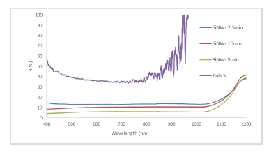 Figure 5: Reflectance of bulk silicon and silicon nanowires (SiNWs).
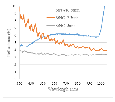 Figure 6: Reflectance of fabricated silicon nanocones (SiNC) compared with SiNW one.
The large index mismath between air and silicon substrate can be reduced by using ergonomic tapered nanostructures which grade the refractive index from silicon to the air. This grading refractive index is ob- served for all nanostructure arrays, specially nanocone arrays. They allow to obtain a volume fraction varia- tion between the top and the bottom of nanocones. Fur- thermore, the nanostructures diffract incoming light and increase the photon path length within the ab- sorber layer.
A comparative study of the electrical properties was also carried out between the bulk monocrystalline silicon, and silicon nanostructures (SiNWs and SiNCs). The surface resistivity called also sheet resistance (Rsheet) permits to evaluate the electrical conductiv- ity of a nanostructured surface. It can be defined as the ratio of the voltage drop per unit length to the sur- face current per width. The common instrument to measure the sheet resistance is the four-point probes method. It consists to apply a current (I) on the outer two probes and to measure the resultant voltage drop (∆V) between the inner two drop. Thus, the sheet re- sistance is calculated by the following equation [14]: Ohm-per-square (Ω/sq) is the measurement unit of the sheet resistance. The resistivity of sample can be defined as the product of their sheet resistance and thickness. According to the results shown in the fig- ures 7 to 9, the sheet resistance of silicon is reduced by Nano structuring the silicon substrate surface. The sheet resistance of 9.143 and 6.997Ω/sq have been obtained for silicon nanowires and silicon nanocores respectively.
A material with a low sheet resistance is better to transfer the electrical charge. Furthermore, the resis- tivity and conductivity can be calculated if the sheet resistance and material thickness are known. This al- lows for the materials to be electrically characterized, by measuring their sheet resistance. Therefore, the electric conductivity of SiNWs and SiNCs (with low sheet resistances) are far better than that of bulk sili- con.
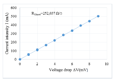 Figure 7: Variation of I(mA) as function of ∆V(mV) of bulk monocrystalline silicon.
![]()
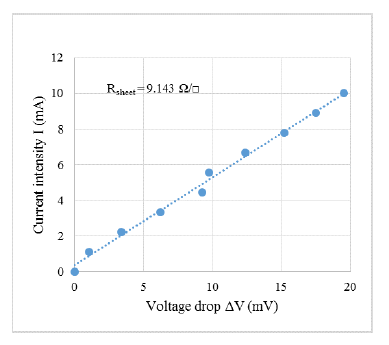 Figure 8: Variation of I(mA) as function of ∆V(mV) of 5-minutes fabricated silicon nanowires.
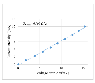 Figure 9: Variation of I(mA) as function of ∆V(mV) of silicon nanocones fabricated by etching 5-minutes processed SiNWs.
5. Conclusion
Silicon nanostructures (SiNWs and SiNCs) have been fabricated by metal-assisted chemical ething. The SEM characterizations have shown that SiNWs fabricated for 5 minutes are vertically straighter than the others. As a result, they exhibit lower reflectance (around 6%) in the 400-1100 nm wavelength range. The SiNCs were also fabricated by etching 5-minutes processed SiNWs. Comparated with SiNWs, SiNCs give the best antireflective properties. They allow to reduce the reflection down to 3% in the 350-1050 nm wavelength range. Measurements and comparison of sheet resis- tances from bulk silicon and silicon nanostructures, have demonstrated an improvement in the property of surface electrical conductivity.
We expect that with high quality surface passivation, performance of solar cells based on these fabricated silicon nanostructures can be greatly enhanced.
- Bilan du Forum Tchernobyl, organis par l’AIEA, l’OMS et le PNUD, septembre 2005
- S. Alexander et Reuters, Fukushima evacuation has killed more than earthquake and tsunami, survey says, NBC News.com, 10 septembre 2013.
- M.A. Green, Y. Hishikawa, W. Warta, et al, Solar cell efficiency tables (version 50), Progress in Photovoltaics 25, 2017, 668-676
- V. K. Sethi, M. Pandey and P. Shukla, Cost Boundary in Silicon Solar Panel, International Journal of Chemical Engineering and Applications, vol. 2, pp. 372-375, 2011.
- Bo Hua, Qingfeng Lin, Qianpeng Zhang and Zhiyong Fan, Efficient photon management with nanostructures for photovoltaics, Nanoscale, 5 2013, 66276640
- H.Wang, K. Lai, Y. Lin, C. Lin, and J. He, Periodic Si nanopillars arrays fabricated by colloidal lithography and catalytic etching for broadband and omnidirectional elimination of Fresnel reflection, Langmuir 26 (15), 2010, 12855-12858
- J. Lui, M. Ashmkhan, B. Wang, and F. Yi, Fabrication and reflection properties of silicon nanopillars by cesium chloride self-assembly and dry etching, Applied Surface Science 258, 2012, 8825-8830
- D. Dimova Malinovska, M. Sendova Vassileva, N. Tzenov, M. Kamenova, Preparation of thin porous silicon layers by stain etching, Thin solid films, vol. 297, pp. 9-12, 1997.
- X. Li, Metal assisted chemical etching for high aspect ratio nanostructures: A review of characteristics and applications in photovoltaics, Current Opinion in Solid State and Materials Science 16, 2012, 7181
- K. Peng, Y. Yan, S. Gao, and J. Zhu, Synthesis of Large-Area Silicon Nanowire Arrays via Self-Assembling Nanoelectrochemistry, Adv. Mater. No. 16, 2002, 1164-1167
- K Peng, Y Yan, S Gao, and J Zhu, Dendrite-assisted grow of silicon nanowires in electroless metal deposition, Advanced functional materials, Vol. 13, No. 2, 2003, 127-132
- T. Shimizu, N. Tanaka, Y/ Tada, Y. Hara, N. Nakamura, J. Taniuchi, K. Takase, T. Ito, and S. Shingubara, Fabrication of nanocone arrays by two step metal assisted chemical etching method, Microelectronic Engineering 153, 2016, 5559
- Z. Huang, N. Geyer, P. Werner, J. De Boor, and U. Gsele, Metal- Assisted Chemical Etching of Silicon: A Review, Adv. Mater., 23, pp. 285-308, 2011
- C. A. Bishop, Process Diagnostics and Coating Characteristics, Vacuum Deposition onto Webs, Films and Foils, 2015
No related articles were found.