Photoluminescence Investigation of Inhomogeneous Porous P-type Si

Adv. Sci. Technol. Eng. Syst. J. 4(3), 190–193 (2019);
 DOI: 10.25046/aj040325
Photoluminescence (PL) of inhomogeneous porous silicon (PS) of p-type is investigated in this contribution. We measured the PL signal at equidistant positions separated by 0.05 mm in area localized between original crystalline Si (c-Si) wafer surface and electrochemically prepared PS layer. Two PL peaks localized at energies 1.8 and 1.9 eV were identified and their parameters were determined. The changes of PL maxima energy (“blue shift”) in dependence on position were observed.
1. Introduction
Researching porous silicon (PS) structures is time-intensive. Extensive collection of results is presented e.g. in [1], but the interpretation of the origin of photoluminescence (PL) signals is still a problem.
Structural characteristics and luminescence of PS prepared by chemical etching were studied by Korsunskaya et al. in [2]. The luminescence spectrum of this type of PS was the result of superposition of two PL bands. The first band represents excitonic recombination in amorphous Si nanocluster smaller than 3 nm. The second band, which prevails at room temperature, is generated by the recombination of charge carriers mediated by the defects in silicon oxide.
Silicon nanocrystallines (NCs) are included in the PS in the form of nanowires on monocrystalline silicon surface composed of different phases of crystalline and amorphous Si. They are covered with oxides (SiOy) and hydrides (SiHx) (Tynyshtykbaev [3]). Authors concluded that the light emission originates in hydride coverages of nanocrystallines. In order to explain the character of PL centers, various models have been elaborated (see e.g. Lenshin [4], experimental analysis of aging effects). The model, in which the maximum of PL localized at 640 nm is related to defective levels os SiHx and SiOy components, is greatly accepted. The presence of groups SiOxHy, observed using FTIR spectroscopy in IR region, was reported in the work [5]. Only small influence of PL on surface morphology was found.
The homogeneity of effective PL from PS was studied by Kayahan [6]. Imaging spectroscopy technique was used by author in order to examine both the effect of atmospheric aging and light illumination applied during anodization process on spatial distribution of PL intensity. He concluded that chemical structure of PS surface plays role in PL and that quantum confinement effect related to surface states can be understood to be a source of luminescence.
Chan [7] observed dependence of energy of PL spectrum on size of pores in PS. Their size was controlled by concentration of HNO3 in etching liquid. Observed “blue shift” of peaks was attributed to quantum confinement effect.
In this work are presented results of our PL experiments on PS. For evaluation of PL signal we used the decomposition procedure based on the fitting of the spectrum by the set of Gaussian peaks. The proper number of the peaks was estimated from the residuum of the fit (Brunner [8]).
2. Experimental Part
The contribution topic is to investigate the PL signal recorded on an inhomogeneous PS sample. The p-type boron doped Si wafers (100) with resistivity of 8 – 10 Ωcm and thickness 600 – 650 nm were used in the experiment. Standard PS was prepared by electrochemical etching process in the solution of HF and MeOH without illumination. Used apparatus is schematically depicted in the Figure 1. Electrical voltage 6V – 11V was applied through mask (Fig. 1) between the exposed area of the Si sample (positive potential) and Pt negative electrode. A constant current of 30 mAcm-2 was maintained during the few minutes of the etching process. The PS was rinsed in ethanol and annealed in nitrogen at 250°C for 30 minutes.
Optical and electrical parameters of PS layer depend on the type and size of the formed crystallites that are controlled by etching process parameters. The mask affects current density in vicinity of their boundary. This shielding effect leads to generation of transient area between exposed and non-exposed part of surface of silicon wafer.
Measurements were performed in this transient area in 17 points separated by 0.05 mm starting from initial crystalline surface (after polishing and cleaning procedures) to prepared PS layer as shown in the Figure 2.
The PL of the sample was measured at ambient temperature. PL spectra were decomposed into Gaussian peaks (this process is explained in more details in [8, 9, 10]). Usage of Gaussian peaks is suitable for sufficiently homogeneous structures composed of domains (layers). Photon emission is considered as an event which is independent of other emission acts. This independence makes possible to use the central limit theorem, leading directly to the Gaussian profile of the PL peak. The presence of light emitting centers of different types in the sample gives the spectrum composed of a set of Gaussians.
The observed spectra were fitted in order to find parameters of the set of Gaussian functions (energy, intensity and width given as FWHM) and to calculate constant bias. This bias represents both noise and signal offset contribution. Root-mean-square (RMS) value was used in the role of the object function in the fitting process.
The calculated parameters of PL peaks (without bias) were statistically tested using bootstrap method (e.g. [11]) based on measured data set resampling. Confidence intervals of peak parameters were estimated using BCa percentile method (“bias-corrected and accelerated”). This version reduces the requirements on number of the used bootstrap data set. In our calculations we used 500 resampling procedures for each sample. Standard 5% confidence limit was used for confidence intervals.
3. Results and Discussion
Estimation of optimal number of PL peaks during fitting process was based on size of residuum. Figure 3 shows how residuum depends on the number of used peeks. Well visible “knee” indicates the optimal model. This approach is explained in more detail in [8] (but briefly speaking, usage of too small number of peaks omits relevant parts of the PL signal, whereas redundant peaks fit mainly the noise). In this case, two relevant PL peaks were found: ~1.8 eV and ~1.9 eV.
Figures 4 – 6 show dependence of parameters of PL peaks (in successive steps energy, intensity and FWHM). Signal was measured at ambient temperature. The visible dependence of parameters of peaks on the position of the measurement point is attributed to the lateral non-homogeneity of the PS layer in the transition region (Fig. 2). Calculated confidence intervals are slightly non-symmetrical. Possibility to evaluate such data sets is the main advance of the bootstrap method, because the approach based on the normal error distribution would be less effective.
Several trends were observed:
Increase of the PL peak energy in dependence on position of measurement point is visible in Figure 4. We suppose that this may be the consequence of the size effect caused by the etching of nanostructural elements. Namely it is related to the SiOxHy compounds covering the structure’s surface. The presence of the SiOxHy has been confirmed in the works [5, 12] using FTIR spectrometry of the samples of this type in wavenumber range 790-1250 cm-1 (0.098 – 0.155 eV).
A noticeablw changes of power of PL signal in dependence on position of measured point can be seen in Figure 5. This is mainly the consequence of increased thickness of light-emitting PS layer in combination with interference of exciting light during PL experiment, but the size effect (controlling light conversion effectivity) can take place in this process also.
Observed changes of FWHM of peaks 1 and 2 on Figure 6 are close to zero and may be non-significant in comparison with the width of confidence interval. Otherwise the increase of FWHM may indicate the inhomogeneity of the sample.
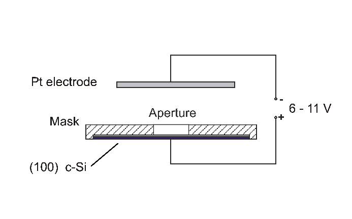 Figure 1: Experimental setup
 Figure 2: Sample geometry and measured area
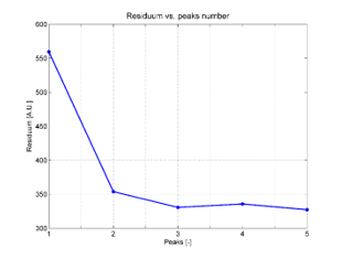 Figure 3: Residuum as a function of number of peaks
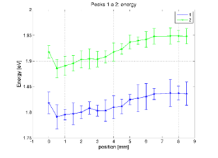 Figure 4: Dependence of energy on the position. Confidence intervals at confidence level α=0.05 are given
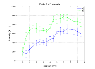 Figure 5: Dependence of intensity on the position. Confidence intervals at confidence level α=0.05 are given
4. Conclusion
Visible increased “blue shift” of both PL maxima (1: at 1.9 eV, 2: at 1.8 eV) occurred in all records in dependence of location of measuring point has been observed. We suppose that this effect is mainly related to the SiOxHy compounds that cover the PS structure’s surface. This structure was modified during preparation of the sample by the non-homogeneous density of the current in transient region (in the vicinity of the mask boundary, see Fig. 1).
The corresponding FWHM of the peak marked as 1 is decreasing, whereas the value of the peak 2 is increasing in dependence on the position of measuring point. These effects are weak, however, the increase of the FWHM parameter may indicate the degradation of the sample homogeneity.
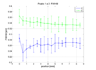 Figure 6: Dependence of width on the position. Confidence intervals at confidence level α=0.05 are given
Conflict of Interest
The authors declare no conflict of interest.
Acknowledgment
The following agencies partly financially supported this contribution: APVV – project No. 15-0152 and VEGA – projects Nos. 1/0900/16, 1/0676/17, 2/1061/18, and 2/0149/18.
- Porous Silicon – from Formation to Application, Volume One, edited by Ghenadii Korotcenkov, CRC Press, Taylor and Francis Group, Boca Raton, London, New York, 2016.
- N.E. Korsunskaya, T.R. Stara, L.Yu. Khomenkova, K.V. Svezhentsova, N.N. Melnichenko, and F.F. Sizov, The nature of emission of porous silicon produced by chemical etching, Semiconductors, 44, 79-83, 2010.
- K.B. Tynyshtykbaev, V. B. Glazman, M.A. Yeleuov, A.T. Isova, B.A. Rakymetov, D. Muratov and S.Z. Tokmoldin, Photoluminescence of Por-Si with High-ordered Mosaic Structure Received at Long Anodic Etching p-Si (100) in the Electrolyte with an Internal Current Source, Optics and Photonics Journal, 3(2B), 217-221, 2013. doi: 10.4236/opj.2013.32B051.
- A.S. Lenshin, V.M. Kashkarov, S.Y. Turishchev, M. Smirnov, E. Domashevskaya, Influence of Natural Aging on the Photoluminescence of Porous Silicon, Technical Physics, 57( 2) , 305–307, 2012.
- M. Kopani, M. Mikula, D. Kosnac, P. Vojtek, J. Gregus, E. Vavrinsky, M. Jergel, E. Pincik: Effect of etching time on structure of p-type porous silicon, Appl. Surf. Sci. 461, 44-47, 2018. doi: 10.1016/j.apsusc.2018.04.228.
- E. Kayahan, Investigation of Photoluminescence Homogeneity Distribution of Nano-Porous Silicon by Imaging Spectroscopy, Journal of Natural and Applied Sciences, 21(3), 738-742, 2017. doi: 10.19113/sdufbed.19374.
- K.S. Chan, Dwight T.J.E, Photoluminescence, morphological and electrical properties of porous silicon formulated with different HNO3 concentrations, Results in Physics 10, 5–9, 2018, https://doi.org/10.1016/j.rinp.2018.04.011.
- R. Brunner, E. Pinčík, H. Kobayashi, M. Kučera, M. Takahashi, J. Rusnák, On photoluminescence properties of a-Si:H-based structures, Appl. Surf. Sci. 256, 5596-5601, 2010. http://dx.doi.org/10.1016/j.apsusc.2010.03.036.
- E. Pincik, R. Brunner, H. Kobayashi, M. Mikula, P. Vojtek, J. Greguš, Z. Zabudla, K. Imamura, P. Švec Jr., The photoluminescence of multicolor silicon, Journal of the Chinese Advanced Materials Society, 4(2), 152-171, 2015- http://dx.doi.org/10.1080/22243682.2016.1151374.
- M. Takahashi, T. Fukushima, Y. Seino, W.-B. Kim, K. Imamura, and H. Kobayashi, Surface Structure Chemical Transfer Method for Formation of Ultralow Reflectivity Si Surfaces, J. Electrochem. Soc. 160(8), H443-H445, 2013. doi:10.1149/2.044308jes.
- B. Efron, R.J. Tibshirani: An Introduction to the Bootstrap. Chapmann&Hall, New York, 1993.
- M. Kopani, M. Mikula, D. Kosnac, J. Gregus, and E. Pincik: Morphology and FTIR spectra of porous silicon, Journal of Electrical Engineering 68, 53-57, 2017. doi: 10.1515/jee-2017-0056.
No related articles were found.