Electronically Tunable Triple-Input Single-Output Voltage-Mode Biquadratic Filter Implemented with Single Integrated Circuit Package

Adv. Sci. Technol. Eng. Syst. J. 6(1), 1120–1127 (2021);
 DOI: 10.25046/aj0601125
This article proposes a compact and simple design of electronically adjustable voltage-mode biquadratic filter using fundamental active cell implemented on a single integrated circuit (IC) package as LT1228. The proposed circuit having triple inputs and single output (TISO) employs namely one resistor and two capacitors as the passive components. All the five possible biquadratic filtering responses, namely low-pass (LP), band-pass (BP), high-pass (HP), band-stop (BS) and all-pass (AP), are realized by the appropriate selection of the relevant input signals. The pole angular frequency and the quality factor of the proposed TISO filter are electronically tunable through the bias current of the IC chip LT1228. Non-ideal effects and sensitivity performance are carried out. The theoretical results are satisfactorily validated by both PSPICE simulation results and experimental measurements using commercially available LT1228.
1.Introduction
Over the decade, analog filters always play a role in many important analog signal processing applications, i.e. communication systems, measurement and instrumentation systems, etc. Nowadays, the realization of an active analog filter using versatile active building blocks has been focused by many researchers due to many advantage features, such as simple circuitry, high linearity, and wide dynamic range. In the literature, many modern active electronic elements have been utilized in analog active filter design, such as current conveyor (CC) [1–7], differential difference current conveyor (DDCC) [8–12], differential voltage current conveyor (DVCC) [13–16], fully differential second-generation current conveyor (FDCCII) [17], current differencing buffered amplifier (CDBA) [18–20], current feedback operational amplifier (CFOA) [21–27], current follower transconductance amplifier (CFTA) [28–29], operational transconductance amplifier (OTA) [30–34], voltage differencing buffered amplifier (VDBA) [35–36], voltage differencing inverting buffered amplifier (VDIBA) [37], fully balanced voltage differencing buffered amplifier (FB-VDBA) [38], voltage differencing transconductance amplifier (VDTA) [39–41], and voltage differencing gain amplifier (VDGA) [42–44]. However, so many of them require at least two or more active elements for their realizations [1–5, 7, 8, 10, 11, 13, 18–27, 30–39, 41, 43, 44]. Moreover, the voltage-mode filters presented in [1–17, 19–29, 38, 42] need a large number of passive resistors, while the articles in [1, 4, 16, 22] also contain three passive capacitors. It is also to be emphasized that the realizations of [1–27] suffer from the lack of electronic tuning capability of their important parameters. Even though some similar works were developed by based on various active building blocks in either bipolar junction transistor or (BJT) or complementary metal oxide semiconductor (CMOS) technologies, they are not commercially available chips and reachable in general. Besides, the performances of the research developments in [1–4, 7–20, 22, 24, 25, 28–37, 39–44] have been demonstrated through only simulation results.
In this communication, an electronically tunable voltage-mode biquadratic filter with three input and one output terminals (TISO) consisting of only single active IC package LT1228, one resistor and two capacitors is introduced. The proposed TISO filter can realize the five standard biquadratic filtering responses, namely low-pass (LP), band-pass (BP), high-pass (HP), band-stop (BS) and all-pass (AP), all at a single output terminal without modifying a circuit structure. It also provides an electronic adjustability of its pole angular frequency (wo) and quality factor (Q) via the external bias current of the LT1228 IC chip. The theoretical propositions are confirmed by PSPICE simulations with LT1228’s model parameters, and the simulated results corroborate the theory. In addition, all conclusions discussed in this work are also verified by the measurement results of an experimentally test circuit with a single IC package LT1228, and the experimental findings are found to be in agreement with the theoretical values.
2. Description of IC Package LT1228
Our design utilizes only one active cell of a commercially available IC LT1228 from Linear Technology Company [46]. An active cell LT1228 is internally a combination of an operational transconductance amplifier (OTA) and a current feedback operational amplifier (CFA) in 8-pin IC package, as demonstrated in Figure 1. This device has three high impedance input terminals (p, n, and z), and one low impedance output terminal (o). It provides the output current iz at intermediate terminal z which is the difference of two input voltages vp and vn (vp – vn) multiplied by transconductance gain (gm). An external impedance Zz is connected to the terminal z, and the potential vz developed across Zz will transfer to the output voltage vo at the terminal o by the CFA. Its ideal terminal characteristics can be described as:
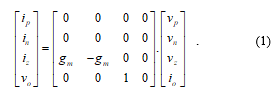 Thanks to the LT1228 manufacturing, the gm-value can be altered to the desired value through the external DC bias current IB by the following relation: [46]
![]()
 Figure 1: IC device LT1228.
(a) active elements in LT1228 (b) schematic representation
(c) equivalent circuit.
3. Proposed TISO Biquadratic Filter
The realization of an electronically tunable TISO voltage-mode biquadratic filter is given in Figure 2. The proposed TISO filter is implemented with a single LT1228 together with one resistor and two capacitors. A straightforward analysis of the proposed TISO filter reveals the following output voltage function:
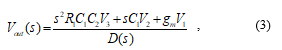 where the denominator D(s) is found to be:
![]() From an inspection of Equations (3)-(4), it appears the five standard biquadratic filter functions can be obtained all at the terminal vout of the proposed circuit by the following conditions.
From an inspection of Equations (3)-(4), it appears the five standard biquadratic filter functions can be obtained all at the terminal vout of the proposed circuit by the following conditions.
- The LP response is obtained by setting vin = v1 (input voltage signal) and v2 = v3 = 0 (grounded).
- The BP response is obtained by setting vin = v2 and v1 = v3 = 0.
- The HP response is obtained by setting vin = v3 and v1 = v2 = 0.
- The BS response is obtained by setting vin = v1 = v3 and v2 = 0.
- The AP response is obtained by setting vin = v1 = –v2 = v3.
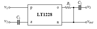 Figure 2: Proposed electronically tunable TISO biquad implementation employing single LT1228.
Therefore, the proposed TISO filter of Figure 2 does not require any element matching conditions or equality constraints for the desired filter function realizations. In all types, the important characteristics wo, and Q are respectively found as: In case of practical design, if C = C1 = C2, then the wo and Q simplify to:
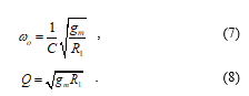
In view of the above expressions, the parameters wo and Q of the proposed TISO filter can be altered electronically by means of gm-value. According to Equation (2), the gm variation can be obtained by an adjustment of the bias current. Also note that since the major contribution of this work is to design a compact and minimum configuration voltage-mode TISO filter with electronic tunability, an orthogonal control of wo or Q is not expected.
4. Non-Ideal Analysis and Sensitivity Performance
In consideration of the non-ideal behavior, the terminal behaviors of LT1228 can be rewritten as:
 where a = (1 – egm) and b = (1 – ev), where |egm | << 1 and |ev | << 1 are the transconductance inaccuracy and the voltage transfer error, respectively. Taking this effect into account, the characteristics wo and Q given in Equations (5) and (6) are modified to:
 In this case, all sensitivity coefficients of wo and Q with respect to the active and passive components are derived and found to be as follows:
 It is clear from Equations (12)-(15) that the absolute values of the wo– and Q-sensitivities are all equal to 0.5. These values ensure that the sensitivity performance of the circuit is to be of low value.
5. Simulation Results
In this section, the proposed circuit and its filtering responses are simulated and discussed through the PSPICE simulation program. For ideal simulation, the LT1228 macro-model parameters obtained from Linear Technology Company and DC supply voltages of ±5V were employed. To demonstrate the functionality of the proposed filter, the circuit is designed for fo = 159.15 kHz and Q = 1. In this case, the various component values have been set as IB = 100 μA for gm = 1 mA/V, R1 = 1 kΩ and C1 = C2 = 1 nF. The simulation results for all filter responses are shown in Figures 3-7, which demonstrates very close agreement with the theoretical responses. For time-domain responses, a 159-kHz sine-wave input voltage with 50 mV peak amplitude was applied to the filter. The simulation results show that the error in fo-value was found to be less than 1%.
 Figure 3: Ideal and simulated LP characteristics
(a) time-domain responses (b) frequency responses
 Figure 4: Ideal and simulated BP characteristics
(a) time-domain responses (b) frequency responses
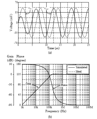 Figure 5: Ideal and simulated HP characteristics
(a) time-domain responses (b) frequency responses
 Figure 6: Ideal and simulated BS characteristics
(a) time-domain responses (b) frequency responses
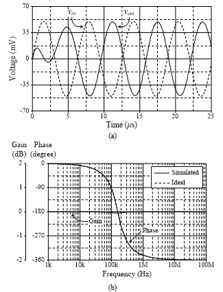 Figure 7: Ideal and simulated AP characteristics
(a) time-domain responses (b) frequency responses
Furthermore, the electronic tuning of gain characteristic for BP filter concerning IB is observed. The related gain expressions of the proposed BP filter, as shown in Figure 8, are plotted for IB = 50 μA, 200 μA, and 500 μA, which resulted in gm = 0.5 mA/V, 2 mA/V, and 5 mA/V, respectively. From Figure 8, the simulation conditions, and corresponding theoretical and simulated fo and Q are summarized in Table 1.
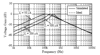 Figure 8: Ideal and simulated frequency responses of the proposed BP filter
with an adjustment of IB.
6. Experimental Results
To further validate the practical workability of the TISO biquadratic filter in Figure 2, the prototype circuit built with readily available IC element LT1228 and discrete passive elements were used to execute experimentally laboratory tests. The circuit was measured using Keysight EDUX1002G digital storage oscilloscope. All of the measured results were performed
Table 1: fo and Q adjustment of the proposed filter by varying IB
| IB (μA) | gm (mA/V) | R1 (kΩ) | C (nF) | Q | fo (kHz) | % fo deviation | |
| Simulated | Ideal | ||||||
| 50 | 0.5 | 1 | 1 | 0.7 | 111.43 | 112.54 | 0.99 |
| 100 | 1 | 1 | 1 | 1 | 157.70 | 159.15 | 0.91 |
| 200 | 2 | 1 | 1 | 1.4 | 222.84 | 225.08 | 0.99 |
| 500 | 5 | 1 | 1 | 2.2 | 352.37 | 355.88 | 0.99 |
at symmetrical supply voltages of ±5 V, and IB = 100 μA (gm = 1 mA/V), R1 = 1 kΩ, and C1 = C2 = 1 nF. This results in fo = 159.15 kHz and Q = 1. To observed transient response, the measurement was carried out with a 159-kHz sine-wave signal input of 50 mV peak amplitude. The experimental results for the transient and frequency responses as well as the associated frequency spectrums are displayed in Figures 9-13. Also from Figures 9(c)-13(c), the measured results of the percentage total harmonic distortion (%THD) of the vout for each filtering responses are noted in Table 2. It can be concluded that the measured results are close to the theoretical analysis, and also verify the functionality of the proposed circuit.
Table 2: Total harmonic distortions of vout in Figure 2.
| Filter | THD (%) | |
| LP | 0.67 | |
| BP | 4.47 | |
| HP | 0.73 | |
| BS | 2.4 | |
| AP | 0.32 |
Another set of measurements have been carried out to examine the electronic adjustability of the proposed TISO filter. BP filter response is used for illustrative purposes. Figure 14 illustrates the measured BP frequency responses for various bias current IB. The gm-values of the considered filter have been set as 0.5 mA/V, 2 mA/V, and 5 mA/V, for IB = 50 μA, 200 μA, and 500 μA, respectively. As follows from Equations (5) and (6), the fo values have been obtained as 112.54 kHz, 225.08 kHz, and 355.88 kHz, while the Q values have been obtained as 0.7, 1.4, and 2.2, respectively.
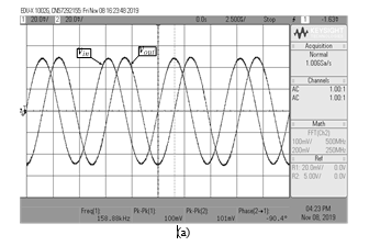
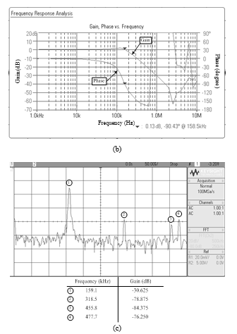 Figure 9: Experimental results of the proposed LP filter.
(a) time-domain responses (b) frequency responses
(c) frequency spectrum
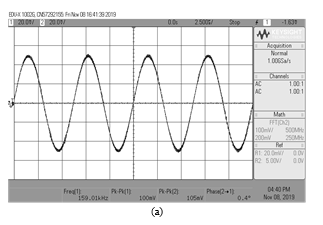
 Figure 10: Experimental results of the proposed BP filter
(a) time-domain responses (b) frequency responses
(c) frequency spectrum

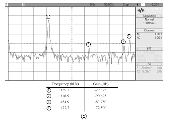 Figure 11: Experimental results of the proposed HP filter
(a) time-domain responses (b) frequency responses
(c) frequency spectrum
 Figure 12: Experimental results of the proposed BS filter
(a) time-domain responses (b) frequency responses
(c) frequency spectrum
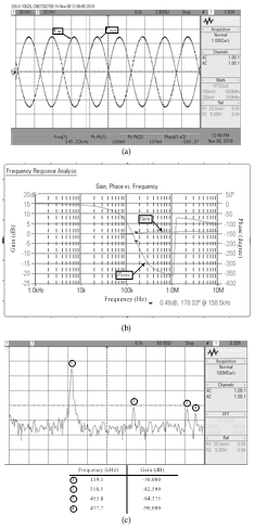 Figure 13: Experimental results of the proposed AP filter
(a) time-domain responses (b) frequency responses
(c) frequency spectrum
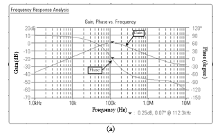
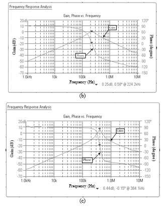 Figure 14: Measured gain responses for the proposed BP filter
with an adjustment of IB.
(a) IB = 50 μA (b) IB = 200 μA (c) IB = 500 μA
7. Conclusions
This contribution describes the practical implementation of an electronically tunable voltage-mode biquadratic filter with triple input terminals and single output terminal. The proposed filter employs only a single commercially available IC LT1228 together with one resistor and two capacitors. The filter can realize all five standard biquadratic filtering functions all at a single output terminal by an appropriate input signal selection. The characteristics of ωo and Q can be controlled electronically and linearly in an electronic manner via the external bias current. Simulation results obtained from the PSPICE macro-model of the LT1228 by Linear Technology as well as constructed in prototype hardware using commercially available IC LT1228 are performed to confirm the properties of the proposed circuit.
Conflict of Interest
The authors declare that they have no conflict of interest.
Acknowledgment
This work was supported by the Faculty of Engineering, King Mongkut’s Institute of Technology Ladkrabang (KMITL) under the contract number 2563-02-01-002.
- M. Higashimura, “Realisation of voltage-mode biquads using CCIIs” Electron. Lett., 27(15), 1345–1346, 1991. https://doi.org/10.1049/el:19910847
- A.M. Soliman, “Kerwin-Huelsman-Newcomb circuit using current conveyors” Electron. Lett., 30(24), 2019–2020, 1994. https://doi.org/10.1049/el:19941368
- M. Higashimura, Y. Fukui, “Universal filter using plus-type CCIIs” Electron. Lett., 32(9), 810–811, 1996. https://doi.org/10.1049/el:19960518
- J. W. Horng, J. R. Lay, C. W. Chang, M. H. Lee, “High input impedance voltage-mode multifunction filters using plus-type CCIIs” Electron. Lett., 33(6), 472–473, 1997. https://doi.org/10.1049/el:19970297
- C. M. Chang, M. J. Lee, “Voltage-mode multifunction filter with single input and three outputs using two compound current conveyors” IEEE Trans. Circuits Syst.-I: Fundamental Theory and Applications, 46(11), 1364–1365, 1999. https://doi.org/10.1109/81.802827
- J. W. Horng, “Voltage/current-mode universal biquadratic filter using single CCII+” Indian J. Pure & Appl. Phys., 48(10), 749–756, 2010.
- J. W. Horng, Z. R. Wang, C. C. Liu, “Voltage-mode lowpass, bandpass and notch filters using three plus-type CCIIs” Circuits and Systems, 2(1), 34–37, 2011. https://doi.org/ 10.4236/cs.2011.21006
- J. W. Horng, W. Y. Chiu, H. Y. Wei, “Voltage-mode highpass, bandpass and lowpass filters using two DDCCs” Int. J. Electronics, 91(8), 461–464, 2004. https://doi.org/10.1080/00207210412331294603
- M. A. Ibrahim, H. Kuntman, O. Cicekoglu, “Single DDCC biquads with high input impedance and minimum number of passive elements” Analog Integr. Circ. Sig. Process., 43, 71–79, 2005. https://doi.org/10.1007/s10470-005-6572-0
- W. Y. Chiu, J. W. Horng, “High-input and low-output impedance voltage-mode universal biquadratic filter using DDCCs” IEEE Trans. Circuits Syst.-II: Express Briefs, 54(8), 649–652, 2007. https://doi.org/10.1109/TCSII.2007.899460
- H. P. Chen, “Universal voltage-mode filter using only plus-type DDCCs” Analog Integr. Circ. Sig. Process., 50, 137–138, 2007. https://doi.org/10.1007/s10470-006-9005-9
- W. Y. Chiu, J. W. Horng, “Voltage-mode highpass, bandpass, lowpass and notch biquadratic filters using single DDCC” Radioengineering, 21(1), 297–303, 2012.
- H. P. Chen, S. S. Shen, “A versatile universal capacitor-grounded voltage-mode filter using DVCCs” ETRI Journal, 29(4), 470–476, 2007. https://doi.org/10.4218/etrij.07.0106.0335
- E. Yuce, “Voltage-mode multifunction filters employing a single DVCC and grounded capacitors”, IEEE Trans. Instrum. Meas., 58(7), 2216–2221, 2009. https://doi.org/10.1109/tim.2009.2013671
- W. Tangsrirat, O. Channumsin, “Voltage-mode multifunctional biquadratic filter using single DVCC and minimum number of passive elements” Indian J. Pure & Appl. Phys., 49(10), 703–707, 2011.
- J. W. Horng, “Voltage-mode multifunction bi-quadratic filter employing single DVCC”, Int. J. Electron., 99(2), 153–162, 2012. https://doi.org/10.1080/00207217.2011.623268
- F. Kaçar, A. Yeşil, “Voltage mode universal filters employing single FDCCII” Analog Integr. Circ. Sig. Process., 63, 137–142, 2010. https://doi.org/10.1007/s10470-009-9440-5
- K. N. Salama, A. M. Soliman, “Voltage mode Kerwin-Huelsman-Newcomb circuit using CDBAs” Frequenz, 54(3–4), 90–93, 2000. https://doi.org/10.1515/FREQ.2000.54.3-4.90
- W. Tangsrirat, T. Pukkalanun, W. Surakampontorn, “CDBA-based universal biquad filter and quadrature oscillator” Active and Passive Electron. Components, 2008, (247171, 6 pages), 2008. https://doi.org/10.1155/2008/247171
- J. Pathak, A. K. Singh, R. Senani, “New voltage mode universal filters using only two CDBAs” ISRN Electronics, 2013(12), (987867, 6 pages), 2013. https://doi.org/10.1155/2013/987867
- S. I. Liu, D. S. Wu, “New current-feedback amplifier-based universal biquadratic filter” IEEE Trans. Instrum. Meas., 44(4), 915–917, 1995. https://doi.org/10.1109/19.392891
- J. W. Horng, M. H. Lee, “High input impedance voltage-mode lowpass, bandpass and highpass filter using current-feedback amplifiers” Electron. Lett., 33(11), 947–948, 1997. https://doi.org/10.1049/el:19970618
- J. W. Horng, “New configuration for realizing universal voltage-mode filter using two current feedback amplifiers” IEEE Trans. Instrum. Meas., 49(5), 1043–1045, 2000. https://doi.org/10.1109/19.872927
- N. Shah, M. F. Rather, S. Z. Iqbal, “CFA-based three input and two outputs voltage-mode universal filter” Indian J. Pure & Appl. Phys., 43(8), 636–639, 2005.
- S. Topaloglu, M.Sagbas, F.Anday, “Three-input single-output second-order filters using current-feedback amplifiers” Int. J. Electron. Commun. (AEÜ), 66(8), 683–686, 2012. https://doi.org/10.1016/j.aeue.2011.12.009
- V. K. Singh, A. K. Singh, D. R. Bhaskar, R. Senani, “New universal biquads employing CFOAs” IEEE Trans. Circuits Syst.-II: Express Briefs, 53(11), 1299–1303, 2006. https://doi.org/10.1109/TCSII.2006.882345
- S. F. Wang, H. P. Chen, Y. Ku, P. Y. Chen, “A CFOA-based voltage-mode multifunction biquadratic filter and a quadrature oscillator using the CFOA-based biquadratic filter” Appl. Sci., 9(11), 2019. https://doi.org/10.3390/app9112304
- W. Tangsrirat, “Novel Current-mode and voltage-mode universal biquad filters using single CFTA” Indian J. Eng. Mater. Sci., 17(2), 90–104, 2010.
- J. Sirirat, W. Tangsrirat, W. Surakampontorn, “Voltage-mode electronically tunable universal filter employing single CFTA” in 2010 International Conference on Electrical Engineering/Electronics, Computer, Telecommunications and Information Technology (ECTI-CON), Chiang Mai, Thailand, 2010.
- R. Nawrocki, U. Klein, “New OTA-capacitor realisation of a universal biquad” Electron. Lett., 22(1), 50–51, 1986. https://doi.org/10.1049/el:19860034
- J. Wu, E. I. E. Masry, “Universal voltage- and current-mode OTAs based biquads” Int. J. Electronics, 85(5), 553–560, 1998. https://doi.org/10.1080/002072198133842
- J. W. Horng, “Voltage-mode universal biquadratic filter using two OTAs” Active and Passive Elec. Comp., 27, 85–89, 2004. https://doi.org/10.1080/0882751031000116160
- M. Kumngern, M. Somdunyakanok, P. Prommee, “High-input impedance voltage-mode multifunction filter with three-input single-output based on simple CMOS OTAs” in 2008 International Symposium on Communications and Information Technologies (ISCIT), Lao, China, 2008. https://doi.org/10.1109/ISCIT.2008.4700228
- J. Sarasri, B. Knobnob, M. Kumngern, “Electronically tunable voltage-mode universal filter using simple OTAs” in 2011 IEEE International Conference on Computer Science and Automation Engineering (CSAE), Shanghai, China, 2011. https://doi.org/10.1109/CSAE.2011.5952912
- F. Kaçar, A. Yesil, A. Noori, “New CMOS realization of voltage differencing buffered amplifier and its biquad filter applications” Radioengineering, 21(1), 333–339, 2012.
- J. Pimpol, N. Roongmuanpha, W. Tangsrirat, “Low-output-impedance electronically adjustable universal filter using voltage differencing buffered amplifiers” in 2019 International Conference on Informatics, Environment, Energy and Applications (IEEA), Osaka, Japan, 2019. https://doi.org/10.1145/3323716.3323738
- O. G. Sokmen, S. A. Tekin, H. Ercan, M. Alci, “A novel design of low-voltage VDIBA and filter application” Elektronika Ir Elektrotechnika, 22(6), 51–56, 2016. https://doi.org/10.5755/j01.eie.22.6.17224
- V. Biolkova, Z. Kolka, D. Biolek, “Fully balanced voltage differencing Buffered amplifier and its applications” in 2009 52nd IEEE International Midwest Symposium on Circuits and Systems (MWSCAS), Cancun, Mexico, 2009. https://doi.org/10.1109/MWSCAS.2009.5236157
- J. Satansup, T. Pukkalanun, W. Tangsrirat, “Electronically tunable single-input five-output voltage-mode universal filter using VDTAs and grounded passive elements” Circuits Syst. Signal Process., 32, 945–957, 2013. https://doi.org/10.1007/s00034-012-9492-0
- D. Prasad, D. R. Bhaskar, M. Srivastava, “Universal voltage-mode biquad filter using voltage differencing transconductance amplifier” Indian J. Pure & Appl. Phys., 51, 864–868, 2013.
- W. Tangsrirat, “Linearly tunable CMOS voltage differencing transconductance amplifier (VDTA)” Informacije MIDEM, 49(2), 61–68, 2019. https://doi.org/10.33180/InfMIDEM2019.202
- O. Channumsin, W. Tangsrirat, “SITO-type high-input impedance voltage-mode multifunction filter using single active element” in 2019 5th International Conference on Engineering, Applied Sciences and Technology (ICEAST), Luang Prabang, Laos, 2019. https://doi.org/10.1109/ICEAST.2019.8802603
- N. Roongmuanpha, T. Dumawipata, W. Tangsrirat, “Triple-input single-output electronically controlled voltage-mode biquadratic filter” in 2019 5th International Conference on Engineering, Applied Sciences and Technology (ICEAST), Luang Prabang, Laos, 2019. https://doi.org/10.1109/ICEAST.2019.8802540
- P. Moonmuang, T. Pukkalanun, W. Tangsrirat, “Voltage differencing gain amplifier-based shadow filter: a comparison study” in 2020 6th International Conference on Engineering, Applied Sciences and Technology (ICEAST), Chiang Mai, Thailand, 2020. https://doi.org/10.1109/ICEAST50382.2020.9165352
- N. Roongmuanpha, T. Pukkalanun, W. Tangsrirat, “Three-input one-output voltage-mode biquadratic filter using single VDBA” in 2020 8th International Electrical Engineering Congress (iEECON), Chiang Mai, Thailand, 2020. https://doi.org/10.1109/iEECON48109.2020.229503
- Linear Technology, “100MHz current feedback amplifier with DC gain control”, LT1228 datasheet, 1994.