Phase-Adjusted Microwave Oscillators Based on a Discriminator
 , Yuri Alekseevich Kazantsev, Sergey Nikolaevich Mikhalin
Adv. Sci. Technol. Eng. Syst. J. 6(3), 319–325 (2021);
 DOI: 10.25046/aj060336
At the conference “System timing, shaping and signal processing” “SYNCHRONO-2020” there was report: “Simulation of steady state microwave oscillator with dielectric resonator” and “Microwave generators, driven by voltage-based microassemblies with dielectric resonators”. An algorithm for calculating a generator with an open dielectric resonator is described. Based on the DesignLab 8.0 simulation environment, the analysis of the stationary mode of generators with electric control (voltage) of the oscillation frequency with parallel and serial feedback circuits is carried out. Analysis of the characteristics of the developed generators in the X-band of voltage-controlled oscillators (VCO) indicated the prospects for using a device with sequential feedback, characterized by a lower level of phase noise (depending on the frequency tuning range, having values from minus 85 to minus 95 dB/Hz when tuning from the generation frequency by 10 kHz). However, this noise level is significantly (by 15…20 dB) worse than world analogues in this frequency range (the C and X frequency ranges are considered). The purpose of creating the device is to use it in generators with analog phase frequency adjustment based on a frequency discriminator. This article describes the characteristics of the VCO and calculates the topology of the phase locked loop (PLL) circuit based on a discriminator formed by a high-quality open dielectric resonator. Such a technical solution is promising as stable generators alternative to highly stable free oscillator. The prototype of the generator under consideration described in the work of A.V. Gorevoy.
1. Introduction
The variant of constructing the topology of a generator with analog phase frequency adjustment (equivalent PLL) based on a frequency discriminator are considered in article. The device is constructed using an oscillator with electrical frequency tuning by changing the constant voltage on a varactor diode embedded in an oscillating system that includes an open dielectric resonator (DR).
The feature of the given design solution and the achieved electrical characteristics of the VCO is the use of the Russian element base: an active element, a varactor diode, a dielectric resonator, dielectric substrates, etc. Among the variants of the active elements of the VCO ‒ complete hybrid-integrated microwave chips produced by Planeta-IRMIS LLC, St. Petersburg, and the hybrid-monolithic integrated circuit (HMIC) model M411154-1 produced by SRC «Istok» named after Shokin, Russia, Moscow region, Fryazino-town − the last one was selected. In this case, the oscillator is designed according to a scheme with sequential (internal) feedback based on a field semiconductor structure, which pre-limits (from below) the expected spectral level of phase noise of the generators [1-3]. However, the advantage of this solution is a higher level of output power.
The PLL generator is based on a developed VCO with the use of oscillatory systems based on an open dielectric resonator, the resonant frequency (in the form of a coupling frequency) of which is controlled by changing the capacitance of a varactor diode (VD), electromagnetically coupling with the DR. The electromagnetic coupling is implemented using a segment of a microstrip line (MSL) − a microstrip resonator (MSR), electromagnetically coupled with the DR and galvanically connected to the VD [4]. The developed design of the VCO uses a varactor diode KA611A-5,B (in the configuration 026 (11) – “cot”). DR [5] with a Q-factor of ~4000 forms by ceramic disk with a relative permittivity of ~40, with a diameter of 5 mm and a thickness of 2 mm. Note that the phase noise of the VCO is not determined by the Q-factor DR, but is determined by the quality factor of the vibrating system of the generator which adjusted by insertion loss due to coupling with varactor diode, the quality factor of which does not exceed a few hundred.
VCO is designed on the basis of a simulation algorithm using a combination of well known wave and our developed circuit representations of active and passive components of microwave circuits. This made it possible to implement the process of optimizing the generator parameters [6-8]. VCO was designed in a three-centimeter wavelength range based on the upper limit of the active element’s working area.
The PLL circuit topology is based on the results of the studies given in [9], calculated using matrix representations [10] of microwave circuits with DR.
2. Main part
2.1. Voltage-controlled oscillator
The PLL generator is designed on the basis of a voltage-controlled generator, which, in turn, is built according to the scheme with sequential (internal) feedback according to the topology shown in Figure 1.
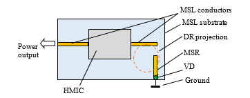 Figure 1: Topology of the VCO on the HMIC of model M411154 (power circuits are not shown)
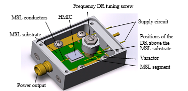 Figure 2: Oscillator with internal feedback (the cover is removed)
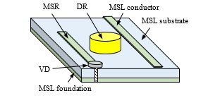 Figure 3: Oscillatory system DR-MSR-VD − frequency-tunable circuit
The design of the VCO is shown in Figure 2, and the circuit topology of the oscillatory system of such VCO coincide to the standard technical solution [4], which is shown in Figure 3. However, as shown by the research, the direct application of such a topology, which is characterized by the presence of a direct (bypassing the DR) electromagnetic coupling between the VD and the MSL segment, worsens the spectral characteristics of the oscillator and limits the range of frequency tuning of the VCO. These characteristics can be improved using the topology shown in Figure 1. Here, the use of orthogonal placement of the MSL and MSR conductors excludes a direct coupling between the VD and the input of HMIS. Designed oscillator with the PLL is based on a block structure. Each block of a certain functional purpose represents an independent technical solution, and the combination forms a VCO with a PLL. The external appearance of the VCO is shown in Figure 4, and the internal structure of the device is shown in Figure 5.
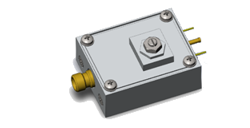 Figure 4: Appearance of the VCO with internal feedback
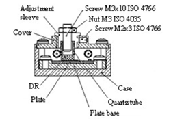 Figure 5: Internal structure of the voltage-controlled oscillator design
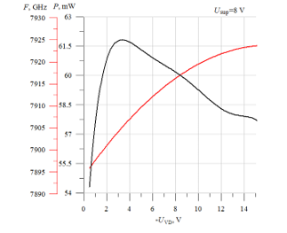 Figure 6: Dependences of frequency and output power of VCO on HMIC of M411154-1 model versus the voltage on the varactor UVD
In the process of creating the device, we studied the VCO with sequential feedback for a number of central frequencies in the C- and X- bands. Typical dependences of the VCO characteristics on the supply and control voltages, as well as the ambient temperature, typical for generators with DR on the chip on HMIC model M411154-1 at all frequency points, are shown in Figures 6-8.
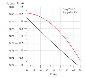 Figure 7: Dependences of frequency and output power of VCO on HMIC of M411154-1 model versus the environment temperature
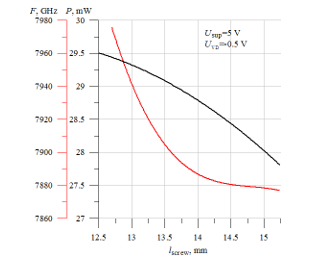 Figure 8: Dependence of frequency and output power of VCO on HMIC on the M411154-1 model versus the relative position of the screw for mechanical frequency tuning lscrew(voltages: of power supply Usup=5.0 V; on varactor UVD=−0.5 V)
Note that the dependence of the generation frequency on the voltage change on the varactor qualitatively repeats the form of the calculated curves. The change in the output voltage is not estimated by calculation, but does not exceed 10%. As can be seen from Figure 8, the output power level depends on the frequency of the DR (or the communication frequency of the DR – MSR system), that is, on the electrical length between the connection point of the DR and the output of the HMIC chip.
Different frequencies VCO have the same appearance Figure 4 and sizes. This VCO differ in the resonant frequency of the DR (and, accordingly, the frequency of the MSR). The same frequency letter of the VCO can operate at different supply voltage of the HMIC, the range of possible values of which is from 5 V to 10 V. A change in the supply voltage is accompanied by a change in the output power. Changing the voltage by 50% causes the output power to double. At the same time, the VCO operates steadily at all voltage values in this range. The upper limit of the supply voltage of the VCO is limited to the maximum permissible value of the supply voltage of the HMIC and it is 10 V. The output power of the VCO varies from 25 to 60 mW in the frequency range from 7 to 11 GHz. The operating current of the VCO supply is from 45 to 50 mA, the efficiency is from 11% (at Usup=5 V) up to 10% (at Usup=10 V).
Confirmed according to the manufacturer property HMIC model М411154-1 decrease of the spectral density of phase noise with increasing voltage, amounting to about minus 2 dB/Hz with increasing the supply voltage at 1 V. The spectral density of phase noise VCO with internal feedback is almost independent of the frequency within the operating range of the chip. The observed deterioration of the spectral power density of phase noise in the VCO when the central frequency changes from 9.67 GHz (the level was minus 96 dB/Hz when tuning from the carrier at 10 kHz) to 10.045 GHz (the level was minus 90.5 dB/Hz when tuning from the carrier at 10 kHz) is determined by the properties of the oscillatory system at these frequencies (Figure 9).
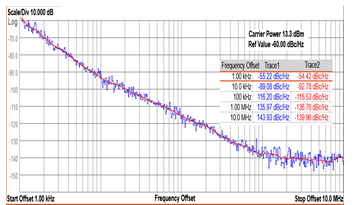 Figure 9: One-Way Phase noise, dB/Hz
From the point of view of the functional purpose of the created VCO, namely, the formation of a phase frequency adjustment system, such a change in the level of spectral density of phase noise is not critical. Note that the achieved values of the phase noise level correspond to a weak connection of the VD with the DR (small insertion loss), which corresponds to a small (0.1%…0.15%) range of adjustment of the “working” frequency of the oscillatory system. When the frequency tuning range (range of coupling and generation) is tripled, the phase noise level increases to minus 83…85 dB/Hz when the carrier frequency is tuned to 10 kHz.
2.2. VCO temperature characteristic
Focusing on the creation of an oscillator using PLL, the characteristics of the spectral density of phase noise of the VCO noted above should be evaluated in conjunction with the possible temperature shift of the generation frequency allowed for its development by the PLL ring. Therefore, an important characteristic for the VCO is the temperature frequency coefficient (TCF), which determines the necessary range of electrical adjustment of the generation frequency to maintain the operation of the automatic frequency adjustment ring.
It is obvious that with the growth of the TCF and, accordingly, the expansion of the necessary frequency range of the VCO frequency adjustment, the phase noise of the VCO increases. The solution of the problem of thermal stabilization of the frequency of generation in VCO devices completely repeats the methods of thermal stabilization of free-oscillator with DR. The main action is to apply thermal compensation of frequency shifts formed by the entire set of frequency-dependent elements of the oscillator design, the opposite shift of the frequency of the DR (in the VCO − it is coupling frequency of the oscillatory system DR-MSR-VD). Thermal compensation can be provided by the correct choice of the TCF resonant frequency DR, that is the temperature coefficient of the relative permittivity of its ceramic material. However, this technique does not provide smooth adjustment of TCF DR and, accordingly, technology adjustment of TCF VCO in the process of regulating the resonance frequency of the DR. To adjust TCF DR (and VCO in General), you can use the dependence of the resonant frequency of the DR on the distance to the metal inclusion (for example, the end of the screw).
Unacceptable lack the engineering solution to the problem of thermal compensation of the frequency shifts of the oscillator with a DR (DRO), based on the influence of the position of the end face of the screw (frequency) at TCF DR (and the generator in General) is the simultaneous effect of the selected position adjusting screw at the resonant frequency of the PD and its temperature characteristics. This problem is solved in the design of the temperature compensator [11] (Fig. 10). Here, practically independent control of the parameters: TCF of the generator and its frequency – is achieved. In such a design, independent control of the parameters of the DR (Fig. 10, pos. 3) ensures its position on the dielectric substrate 1 (on the one of its side), which is located in a close metal cavity 2 (generator housing). DR 3 the electromagnetically-coupled with strip line segment 4 (not visible) which connected to the active element 5. The effect of independent control of the parameters of the DR 3 is provided by the below-cutoff waveguide 7. The segment of the circular waveguide 7 is mounted in cover 10 of the cavity 2 with a possibility to movement coaxially on the opposite to DR 3. There are moveable short-circuitor 8 is mounted on the one end of the waveguide 7. On another end of the waveguide 7 fixed installed the dielectric disk 9. The diameter, relative permittivity and thickness of dielectric disk 9 are determined by special calculated ratios taking into account the properties of DR 6. The second DR 6 is mounted of the disk 9 surface facing to DR 3, DR 6 TCF is opposite in sign to the TCF of DR 3. The control of TCF of DRO is provided by a variation of TCF of the coupling frequency of the system of two coupled DR 3 and 6.
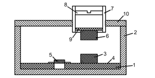 Figure 10: The thermal compensation system of DRO frequency shift
The frequency of the generator is adjusted through a series of adjustments and their combination.
The displacement of the movable short-circuitor 8 in the circular below-cutoff waveguide segment 7 causes a change of the own resonant frequency of DR 6. In this case, the following change of electromagnetic coupling of DR 6 with the first DR 3, and so and the change of the coupling resonant frequency, that’s controls to the oscillation frequency, and the temperature coefficient of the frequency in our oscillator. In the similar manner, the variation of electromagnetic coupling between the first 3 and second 6 DR influences upon the oscillator parameters. The coupling change between DRs 3 and 6 is provided by the longitudinal displacement of the circular below-cutoff waveguide segment 7, on which the second DR 6 is mounted. The various influences of these two retuning elements upon the frequency of the generated oscillations and on its TCF permits to perform its independent adjustment. We would like to note that the TCF tuning of such an oscillatory system represents a regression process and requires a number of iterations provided in several stages.
Nevertheless, at reaching of the required result, the constructive relationships, which provide the required oscillator parameters, are enough confidently reproduced in the series of devices, for example, in the production of Figure 11.
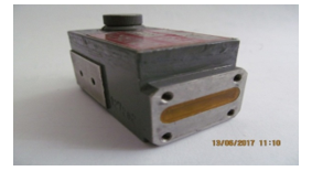 Figure 11: X-band VCO with the thermal compensation system of DR
Our experience in developing such a generator with the described design of the oscillatory system shows the possibility of providing a TCF corresponding to temperature shifts of 20 kHz/°C in the temperature range from -40°C to +60°C at a frequency of 10 GHz. However, the described technical solution of the microwave generator has a design disadvantage with obvious advantages. Note, that with the application of the correctly selected TCF DR, it is perhaps to achieve satisfactory TCF VCO value. In the presented version, the temperature shift of the VCO frequency is less than 100 kHz/ºC, which is 10 MHz when the temperature changes by 100ºC. If the ambient temperature range is reduced to 10ºC, the frequency shift range is reduced to 1MHz.
With that said, in our device, the problem of thermal compensation of temperature shifts of the VCO frequency is solved in a complex with thermostating of PLL elements based on Peltier regulators. This made it possible to reduce the required range by varactor frequency tuning to about 3 MHz and thus reduce the level of phase noise by 10 dB.
The given data of the VCO with internal feedback show that it is possible to create generators on the domestic HMIS, the set of parameters of which corresponds to the world level [12].
2.3. Characteristics of the thermostat
Effective stabilization of frequency and the device of the oscillator with PLL as a whole is possible when placing the VCO (or when the block structure of the generator − all its nodes) inside the thermos. Maintaining the set temperature is possible either by liquid cooling (heating), or using Peltier elements. The latter, although it has a lower efficiency, does not contain mechanical components (pump), does not pose a danger to electronic components (in case of media leakage), is absolutely resistant to mechanical influences, and also removes maintenance issues.
A Peltier element, which is a semiconductor wafer with dimensions of 34×30×8 mm, is used for temperature control of a PLL generator with overall dimensions of about 60×50×30 mm (volume V) in the range from +20 to +30°C when the ambient temperature changes from –20 to +60°C. The Peltier element surface is in direct contact with the temperature-controlled object. The radiator removes excess heat from the heating side of the Peltier plate.
The thermostat device, in addition to the Peltier element, contains a temperature sensor, a control circuit, and a power supply – Figure 12.
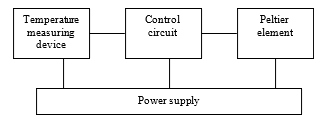 Figure 12: Structural diagram of the thermostat
The temperature sensor is implemented on the TMP01 Analog Devices chip, contains a precision semiconductor thermosensitive element with a reference voltage source (RVS) and two comparators in one 8-pin package and provides temperature measurement accuracy at 1ºC in the temperature range from –55 to +125ºC.
The control circuit is formed by an amplifier and two comparators that set two temperature thresholds, relative to which the control circuit includes heating or cooling the thermostatically controlled object. To create two reference temperature values, an RVS is used – Figure 13.
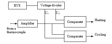 Figure 13: Functional diagram of the temperature control device
The temperature condition of the Peltier element plane is controlled by the current from units of amperes using power transistors, using bridge drivers (they provide current flow through a large load in the required direction, depending on the control signals “Heating” and “Cooling”).
The heat stabilizer is based on integrated circuits TMP01 and L298 and Peltier element for 10 W (maximum current of 3.5 A), which provided temperature maintenance in the range from +20 to +30°C in a thermostatically controlled device with a power consumption of no more than 1 W (power consumption of the VCO ~0.5 W) with a volume V in a given range of ambient temperatures. For demand response to changes in temperature stabilized device power control exceeds the power that “excites” the system, i.e. leads to excessive heating or cooling.
The schematic diagram of the control device contains circuit solutions (Schmitt inverters) designed to increase the stability of the control path in the area of threshold temperatures and prevent multiple switching of the driver due to temperature measurement errors, instability of the reference voltage source, interference effects, etc.
Implementation of the thermos is made using rigid foam (“penoplex”) and has a wall thickness of at least 20 mm (Figure 14).
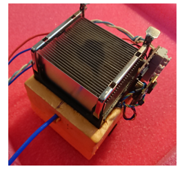 Figure 14: Thermostatic generator
The thermal stabilizer provided stability of the VCO generation frequency better than 1 MHz in the temperature range from –20 to +60°C, which simplifies the requirements for a sufficient range of tuning its frequency less than 2 MHz and thus the level of phase noise of the VCO is not worse than 90 dB/Hz when debugging from the central frequency at 10 kHz.
2.4. The topology of the phase-adjustment loop Calculation
We analyze the construction of the PLL loop based on the phase discriminator on the DR. The principle of constructing such a generator is known [9] (Figure 15), the characteristics are limited by the selective capabilities (the steepness of the phase characteristic) of acceptable design solutions of the DR and, according to A. Gorevoy, are mainly determined by the spectral characteristics of the PLL circuit, which, in turn, depends on the phase noise introduced by the LNA. Based on the estimation of the spectral density parameter of phase noise in the circuit Figure 15 at approximately 150 dB/Hz with a 10 kHz detuning from the generation frequency with the given characteristics of the circuit elements and with phase noise of the VCO of approximately 110 dB/Hz with a 10 kHz detuning from the generation frequency, it is of interest to use the scheme for phase stabilization of the frequency of the developed VCO.
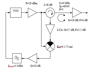 Figure 15: PLL generator with rejecting DR filter
We will evaluate the characteristics of PLL circuit elements when constructing a discriminator based on a DR made of modern ceramic materials with a lower TE01δ oscillation mode, whose own Q-factor exceeds 1000 at a frequency of 10 GHz [5]. In this case, the PLL circuit is organized according to Figure 16.
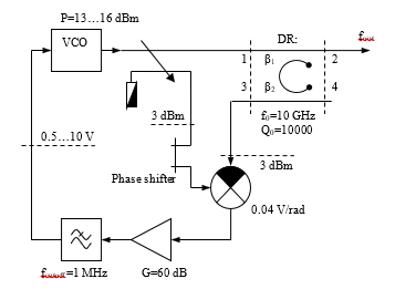 Figure 16: PLL generator with pass band DR filter
In contrast to the circuit of Figure 15, the phase discriminator is formed using a band-pass filter on the DR, represented by a four-pole with ports 1…4. The single-ended phase detector is formed by a hybrid bridge and a HSHS-8202TR1G diode Assembly. The required level of the input signal on the diodes, equal to 2.5 dBm, taking into account the losses in the hybrid bridge of 0.5 dB, is provided by the transmission coefficient of the directional coupler (in our case, minus 10…13 dB) and the transmission coefficient of the filter on the DR (four-pole with ports 1…4). The filter characteristic, i.e. the required coupling coefficients of DR β1 with the input MSL (between ports 1 and 3) and β2 with the output line (between ports 2 and 4) are determined using wave matrices of DR [10], which for the resonant frequency has the form:
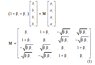 where ai и bi − incident and reflected waves at the entrances i equal 1…4, а a1=13…16 dBm. Taking into account equality a1=−b4, since to the port 4 a quarter-wave open segment of a long line is connected and, in the approximation, a2≈a3≈0 «reflected» wave b3 entrance 4 it is represented by the formula dBm, from which the coupling coefficients β1 and β2 are determined, which are interconnected by the equation
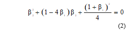 Given the requirement of the maximum loaded Q-factor of DR (minimization of the model coefficient) to the equation (2) satisfy the positive values of relationship coefficients β1=0.05 and β2=0.2. Thus the output device at the resonant frequency level of a wave decreases by 0.17 dB, and the loaded Q-factor will be 8000.
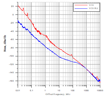 Figure 17: One-Way Phase noise, dB/Hz
Experimentally, it was possible to realize the value of the coupling coefficients, which provided a wave attenuation of 0.5 dB at the resonant frequency of the DR (with a loaded Q-factor of 5500). At the output of the 3 bandpass filter, the wave level was minus 11 dB relative to the level a1. At the output of the phase detector, the voltage is 3…30 mV with a phase change of 45º, which corresponds to a transmission coefficient of 0.04 V/rad.
The obtained characteristics at the points of the phase control circuit correspond to the circuit parameters given in [9], which suggests the possibility of improving the level of phase noise of the developed VCO by 20…25 dB. However, the actual parameters of the PLL generator based on the frequency discriminator were slightly worse than expected, as illustrated in Figure 17. The reason lies in the insufficiently accurate setting of the electrical lengths of the MSL segments of the phase discriminator topology.
3. Conclusion
The results of creating a VCO representing the option of a PLL generator are presented. The properties of the VCO are studied and optimized to ensure phase adjustment of its frequency. There are designed the device for temperature control of the oscillation frequency of the VCO PLL circuit. The options considered for building a PLL circuit based frequency discriminator, educated DR. This method of constructing highly stable oscillators is well known [13], but requires the use of extremely high-quality resonators (Q-factor of about 100,000) to construct a frequency discriminator. But generators with such DR are not suitable for technical use due to poor thermal stability and vibration resistance. Nevertheless, modern ceramic resonators (Q-factor of about 15,000) allow us to achieve an acceptable level of phase noise of generators built on this principle. The algorithm for analytical calculation circuit PLL oscillator voltage controlled on the basis of the frequency discriminator is presented. Physical modeling of the phase discriminator performed based on the calculation results confirmed the reliability of the calculated data.
The process of creating PLL generators with electrical frequency adjustment (or controlled by constant voltage) showed the possibility of successful application of design algorithms for such devices, including phase correction circuits, when the obtained characteristics of the nodes (options) of PLL generators differ within the ranges of technological adjustments.
The Russian element base makes it possible to create devices with parameters at the level of foreign analogues based on palliative technical solutions.
Created on the basis of a domestic active element (produced by NPP «Istok» named after Shokin), a varactor diode (produced by NIIPP Tomsk) and open dielectric resonators (produced by LLC «Keramika», St. Petersburg), the VCO corresponds to the level of foreign analogues in terms of a set of parameters. The use of PLL assumes the possibility of reducing phase noise by 20…25 dB/Hz. In addition, the development involves further improvement of both the parameters of the VCO and the PLL chain based on improving the characteristics of the element base.
Conflict of Interest
The authors declare no conflict of interest.
Acknowledgment
The study is performed with a financial support from the Ministry of Science and Higher Education of the Russian Federation (Unique identifier: RFMEFI60719X0324).
- A.I. Afanas’ev, L.V. Alekseychik, I.I. Brodulenko, N.G. Gavrilyuk, V.A. Maltsev, “Technical condition, development trends and design of stable solid-state generators and low-power microwave filters Reviews on ET,” Series 1, UHF Electronics, 2 (1698), 1993.
- V. Gevorkyan, V. Kochemasov and V. Shadsky,”Generators with the use of dielectric resonators. Part 1,” Electronics. The science. Technology. Business, 2, 114?128, 2020, doi:10.22184/1992-4178.2020.193.2.114.128.
- U. Güttich,”Active Elements Used in Microstrip Dielectric Resonator Oscillators”, Microwave Journal, 4, 92?96, 1996.
- T.N. Narytnik, V.I. Priymak, V.B. Fedorov, “Oscillatory microwave systems with miniature dielectric resonators in amplifying and converting devices,” Electronic equipment, Series 1, 7, Microwave Electronics, 15–21, 1985.
- “RF and UHF ceramic materials and microwave elements”, The catalogue of products of JSC «Ceramica», Sankt-Peterburg, 2004.
- V.M. Gevorkyan and Yu.A. Kazantsev, “Analysis of scattering matrices of UHF devices with the help of equivalent circuits in the software DesignLab 8.0”, Proceedings of MKEEE-2016, 254–256, 2016.
- V.M. Gevorkyan, Yu.A. Kazantsev and S.N. Mikhalin, “Analysis of UHF resonance circuit with electrical frequency control by utilization of the software DesignLab 8.0”, Proceedings of MKEEE-2018, 382–386, 2018.
- Design Procedures for Series and Parallel Feedback Microwave DROs. Stellenbosch University, 2007.
- A. Gorevoy, “A Low Noise Oscillator Based on a Conventional Dielectric Resonator”, Microwave Journal, 11, 84?94, 2013.
- M.E. Ilchenko, V.F. Vzyatyshev, L.G. Gassanov, Yu.M. Bezborodov, M.N. Berger, V.S. Dobromyslov, B.Yu. Kopilevich, T.N. Narytnik, V.B. Fedorov, B.S. Chernii, “Dielectric resonators,” M.: Radio and Communication, 1989
- A.I. Abramenkov, V.M. Gevorkyan and D.A. Kovtunov, “Generator”, Certificate on USSR invention N1653125 dated 01.06.1989. Bull of invent N20 dated 30.05.1991.
- L. Belov, V. Khilkevich, “Generators with dielectric resonators for frequency stabilization,” Electronics: Science, Technology, Business, 7, 54–59, 2006.
- D.P. Zarapkin, “Application of dielectric resonators with waves of the “whispering gallery” type for frequency stabilization of ultrahigh frequency autogenerators,” Radio Engineering, 2, 28–35, 2002.