Advanced Physical Failure Analysis Techniques for Rescuing Damaged Samples with Cracks, Scratches, or Unevenness in Delayering
 , Pik Kee Tan, Siong Luong Ting, Chang Qing Chen, Hao Tan, Naiyun Xu, Krishnanunni Menon, Hnin Hnin Win Thoungh Ma, Kyaw Htin
Adv. Sci. Technol. Eng. Syst. J. 6(4), 52–61 (2021);
 DOI: 10.25046/aj060407
This paper is an extended version of work published in IPFA 2020. In the previous paper, advanced physical failure analysis (PFA) techniques for rescuing damaged samples with cracks, scratches, or unevenness in delayering are introduced. In the present work, the techniques will be further exploited and summarized for the potential applications in general devices. The three typical rescue cases will be fully discussed through comprehensive analysis on the failure mechanism and the rescuing process. Compared to the conventional PFA techniques that normally require back-up samples, the novel rescue techniques offer more alternative solutions for coping with sample damage problems in delayering without starting over with a new sample that would waste machine time and human resources. These new PFA techniques involve only basic failure analysis (FA) skills that could be easily manipulated and FA equipment that is commonly available in FA labs, and would extend the scope and capability of the tradition PFA to help the FA engineers deliver FA results with high quality and high success rate in the daily work, especially for handling “one of a kind” devices.
1. Introduction
Delayering by finger polishing is one of the commonly used physical failure analysis (PFA) techniques in the failure analysis (FA) labs. This technique is simple, direct, and flexible, which is basically mechanical polishing using fingers to press the sample against a rotating cloth plate with polishing slurry in between the cloth and the sample [1]. Before the polishing of each layer, reactive ion etch (RIE) is usually used to expose the metal structure by removing the inter-metal dielectric (IMD) for a faster removal rate and a more even surface of the polished sample. For monitoring the polishing progress, FA engineers will then use the scanning electron microscope (SEM) and the optical microscope (OM) to inspect the sample surface. A typical delayering workflow in PFA is shown in Figure 1. Normal process of the delayering completes when the target layer is reached, followed by the defect identification and analysis. However, if the sample comes with the accidental damage or the naturally generated edge rounding during the delayering, the problems have to be fixed to restore the sample to the former condition before the polishing is continued to the target layer.
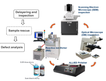 Figure 1: Illustration of a typical delayering workflow in PFA.
The common problems encountered in the delayering include sample cracks, polishing scratches, and surface unevenness [2-6]. The sample cracks refer to the sample die breaking into pieces due to chipping, dropping or crushing, which would pose great challenges to the following polishing if the crack lines extend across the defect area. The polishing scratches on the sample surface are usually caused by aggregated slurry particles mixed in the slurry solution or diamond lapping films when doing pre-polish sample preparation. The surface unevenness of the samples results from the edge effect which is a normal phenomenon in the delayering by both finger polishing and machine polishing [7-10]. For the small targets such as single memory bits or localized hotspot locations from electrical fault isolation (EFI), the unevenness will not lead to severe problem. But for the big inspection area or the defect location at the edge of the sample, the unevenness must be specifically treated to maintain the feasibility of the FA process. These problems could even become worse with the continuous development of the semiconductor devices, which introduces more layer stacks, smaller transistors, and softer low-k dielectrics. Moreover, accidents due to human error are considered inevitable and hard to control in the real FA work place. Hence, compared to the preventive practice for reducing the sample damage in delayering, finding rescue solutions to the problems is a more pressing need.
In the previous studies, sacrificial dummy as a polishing balance, platinum (Pt) as an etching mask, and lateral delayering with adapted polishing plate were used to counteract the edge effect [11-13]. Other studies focused on the impact of pad properties [14-15], cloth roughness [16], slurry particle size [17-18], and interaction mechanism [19-20] on the material removal rate and polishing uniformity. However, the unevenness problems have not been fully resolved because of the complexity of the issue. Unevenness is related to numerous factors such as force of pressing samples, speed of plate rotation, polishing angle, polishing orientation, slurry type and sample thickness, which are all dependent on the experience of the engineers. These variable parameters and different conditions of different devices would make it nearly impossible to operate in a standard procedure. In addition to surface unevenness, polishing scratches and sample cracks in the delayering are also dealt with in the daily FA work, but most of time there is no effective method of bringing the sample back to the normal condition. In order to fill the skill gaps, new techniques need to be developed.
In this paper, we will introduce three advanced PFA techniques for rescuing damaged samples with cracks, scratches, or unevenness in delayering by finger polishing, through their according typical FA cases. The first case uses the diamond lapping film and the sacrificial dummy samples to fix the cracked sample for continuing the FA process with no effect from the cracks. The second case uses e-beam Pt deposited in SEM machine to repair the scratch pits in the region of interest (ROI). With the polishing progresses to the lower layers, the scratch features gradually diminish until thoroughly removed from the sample surface. In the third case, an innovative technique combining controlled slurry polishing and partial RIE was developed for creating an ultra-large inspection area (> 50000 μm2) with negligible unevenness. Compared to the conventional PFA techniques that normally require back-up samples, the novel rescue techniques offer more alternative solutions for coping with sample damage problems in delayering without starting over with a new sample that would waste machine time and human resources. These techniques would extend the scope and capability of the tradition PFA, and help the engineers deliver FA results with high success rate, especially for handling “one of a kind” devices.
2. Experiments
The experiments of the three cases were performed on a 40 nm node logic device, a 40nm node static random access memory (SRAM) device, and a 40 nm node “snake” metal line electrical test (ET) device, respectively. A mechanical polisher (ALLIED HighTech TwinPrep 5) with a rayon flock polishing cloth (ALLIED Spec-Cloth) and 3 μm polishing slurry (ALLIED water based diamond suspension) were used for slurry polishing. A 3 μm and a 15 μm diamond lapping films (ALLIED) were used for the selective polishing on the dummy samples. A SEM system (FEI MagellanTM 400L) equipped with a gas injection system was used for the topography inspection on the sample surface and the e-beam Pt deposition on the scratch pits. An optical microscope (ZEISS Axiotron) was used for the fast inspection during the mechanical polishing and the sample height determination. A RIE system (Corial 200 IL) was used to remove the IMD materials. TEM sample preparation was performed using a FIB-SEM dual-beam system (FEI Helios NanoLab 450S). TEM analysis was performed using a 200 kV Field Emission TEM (JEOL JEM-2100F).
3. Results and Discussion
3.1. Case 1: Using Diamond Lapping Film and Sacrificial Dummy to Save Cracked Sample with Target Defect Area Close to Gaps/Crack Lines
The first case is about a 40 nm node logic device which suffers scan failure with a diagnosed trace path across an area of 283 μm × 71 μm. The sample was delayered halfway (at M8) in the PFA process when it accidentally dropped broken into multiple pieces. Directly continuing the delayering on the piece that contains the defect area would come with the difficulty of polishing and the high risk of missing the defects that could locate anywhere along the whole trace path through each layer. Instead, the broken pieces were glued together with two dummy samples as polishing balance on a substrate using wax (Figure 5a). However, when the normal slurry polishing on the joined sample reached V5, obvious unevenness was observed near the crack line and the wax gap (Figure 5b). The mechanism of the unevenness generating during slurry polishing is illustrated in Figure 2a-2c. The height difference between the dummy sample and the target sample without treatment aggravated with the progress of delayering and caused surface unevenness of the sample.
Figure 3 shows a failed case of delayering where the dummy sample was originally higher than the target sample at M8, according to the focusing conditions in OM. After the sample was delayered from M8 to V5, severe unevenness had generated in the defect area and the dummy side was still higher than the sample side (Figure 3c, 3d), which means that the unevenness would further extend to the lower layers in the following polishing process. In the rescued case, we had to prevent the unevenness from extending to the defect area that would introduce the risk of missing the defect when the defect location or the layers were misjudged due to the unevenness. The unevenness in the defect area also posed great challenges to the layer-by-layer inspection for finding the defects, especially at the critical layers (V5 in this case) which are the interfaces between the low-k IMD layers (M5
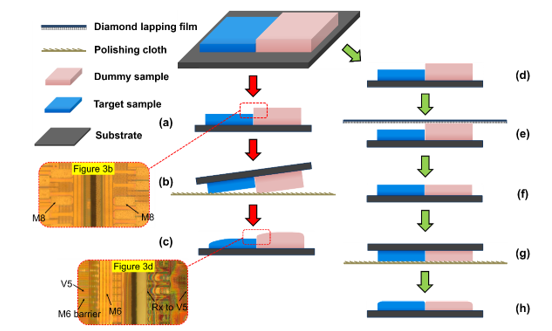 Figure 2: Schematic illustration of the failed case and the successful case of rescuing the cracked samples. (a-c) In the failed case, the height difference between the dummy sample and the target sample without treatment will aggravate with the progress of delayering and induce surface unevenness. (d-h) In the successful case, by using the diamond lapping films to remove the height difference before the polishing, the target sample will achieve an even surface in the defect area which is close to the crack line. Insets are the example OM images from the failed case.
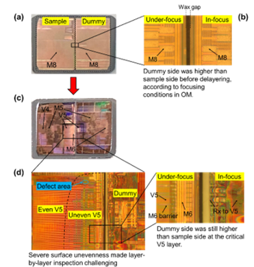 Figure 3: Failed case of delayering where (a) the dummy sample was originally higher than the target sample at M8, according to (b) the sample focusing condition in OM. When the target sample reached V5, (c, d) severe unevenness had generated in the defect area.
and below) and non-low-k IMD layers (V5 and above). Once the sample went with a non-uniform surface at the critical layer, the unevenness would significantly deteriorate due to the great difference (up to 10 times) of the removal rate between the low-k materials and the non-low-k materials. Moreover, the sample inspection and the defect finding in SEM would be tediously prolonged because the defect area may cover multiple layers so that the staggered inspections on the different portions of the different layers in the trace path would have to be performed through repeated polish-and-view processes.
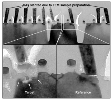 Figure 4: TEM (across PC) images of the target location and the reference location. Damaged Rx and PC-CA short were observed at the target location.
Therefore, with the understanding of the significant effect of the height difference on the FA results, we managed to rescue the sample by using the diamond lapping films to polish down the dummy sample until it was the same height as the target sample. The estimation on height difference was made according to the focusing condition in OM as shown in Figure 5c. The magnification used on the OM was 100× and the numerical aperture (NA) was 0.9. The measurement error regarding to Depth of Field (DOF) was ~ 0.22 μm [21], far smaller than the particle size ~ 3 μm of the polishing slurry. It is worth to mention that the chosen dummy sample should not be thinner than the target sample in the first place.
After removing the height difference between the target sample and the dummy sample, the unevenness was slowly eliminated in the subsequent slurry polishing within the V5 layer (Figure 5d). The sample was restored to its former evenness from V4 downwards, and the defect of damaged Rx and PC-CA short were found at the PC/CA layer (Figure 5e). The mechanism of the rescue process is illustrated in Figure 2d-2h. Figure 4 shows the TEM (across PC) images of the target defect location and the reference location, from which we can see that CA landing on the PC residue caused PC-CA short and the Rx below was damaged. It was suspected that PC residue blocked the PC etching at the defect location. In summary, to rescue the cracked samples with the defect area close to the gap/crack lines, dummy samples as polishing balance need to be used and the surface of the joined samples must be levelled first using diamond lapping films, before the slurry polishing is continued.
3.2. Case 2: Using E-beam Pt Deposition to Repair Scratched Sample with Scratch Pits in the ROI
The second case involved a 40nm node SRAM device. Electrical bench measurement on the failed unit showed source-drain leakage failure in an ET SRAM structure. EFI hotspot analysis was then performed to narrow down the ROI for the root cause finding in PFA. According to the detected defect location, the sample was delayered and viewed from the top layer. To avoid potential unevenness problem subject to the density difference between the target device region and the adjacent scribe lines, the thick top metal layers were removed using 3 μm diamond lapping film. Unfortunately, multiple scratch pits were accidentally created in the ROI during the lapping process (Figure 9a), which would introduce potential damage to the defect. The failure mechanism is illustrated in Figure 6a-6c. The scratch feature as a pit will extend from the scratched layer to the lower layers if the slurry polishing is directly continued without treatment.
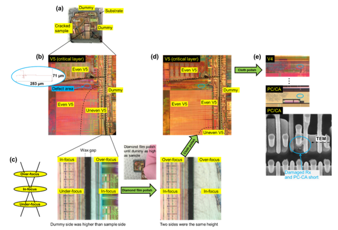 Figure 5: Successful case of sample rescue by using diamond lapping films and sacrificial dummy samples to save the cracked sample with the target defect area close to the crack lines. (a) The cracked samples (halfway at M8) were stuck onto a substrate together with two dummy samples as balance before the slurry polishing is continued. (b) When the joined sample reached V5, obvious surface unevenness was seen near the defect area, generated from the height difference between the dummy sample and the target sample. (c) By selective polishing on the higher dummy side using the diamond lapping films until it was the same height as the target sample, (d) the unevenness was slowly removed in the subsequent slurry polishing within the V5 layer. (e) The sample was restored to its former evenness from V4, and damaged Rx and PC-CA short were found at the PC/CA layer.
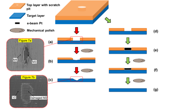 Figure 6: Schematic illustration of the failed case and the successful case of rescuing the scratched samples. (a-c) In the failed case, the scratch feature as a pit will extend to the lower layer if the slurry polishing is continued without treatment, which may damage the defect location. (d-g) In the successful case, by selectively filling the scratch pit with e-beam Pt, the defect location is protected from the damage of over-RIE and over-polish. Insets are the example SEM images from the failed case.
A failed case study is shown in Figure 7, where the sample was scratched at M4 by the diamond lapping films (Figure 7a). A scratch pit as big as 1 μm × 4 μm was generated in the defect area. Since the following slurry polishing evenly abrades any surface topography with feature size larger than 3 μm (average diameter of the slurry particles), the scratched location was over-polished (M2 damaged) and the affected area increased to 3 μm × 5 μm when the sample reached V2 layer (Figure 7b). Larger and deeper scratch pits could even cause more severe problems such as metal smearing short, metal broken or other artifacts. In addition, the local unevenness would induce the difficulty of sample inspection and defect identification. Although we can use the color pattern of the sample surface as an indicator of certain areas being polished more aggressively during the sample viewing in OM, the complicated sample surface condition and the limited image magnification make the judgement on the ROI unreliable.
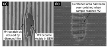 Figure 7: Failed case of delayering where (a) the sample was scratched at M4 by diamond lapping films, and (b) the scratched area had been over-polished when the normal slurry polishing continued and reached V2.
To solve the problem, we used e-beam Pt deposition to fill the scratch pits in SEM. The concept is using Pt metal patch as substitute for Cu to block the RIE and resist the slurry polishing on the next layer. The critical part of this method is the Pt thickness. Over-deposited Pt will leave Pt residue at the ROI resulting in surface unevenness in another way. Therefore, in the beginning we used high kV SEM to deposit thinner Pt film compared to the metal layer of which the thickness was determined by e-beam penetration depth in the SEM imaging. If the Pt were fading faster than the adjacent metal under slurry polishing, we would deposit extra layer of Pt on the ROI. For 40nm node device in this case, the Pt thickness was fixed to 0.1 μm. Voltage of 3 kV and current of 0.8 nA were used for SEM. The deposition rate is 10 μm (length) × 10 μm (width) × 10 μm (thickness) per 10 mins.
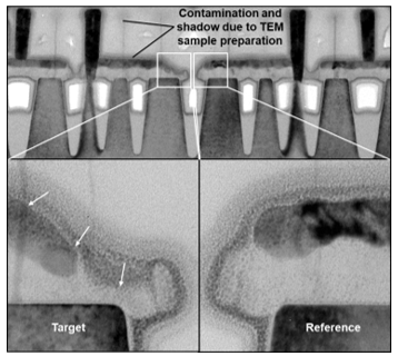 Figure 8: TEM (along PC) images of the target location and the reference location. Abnormal PC/NiSi profile was observed at the target location.
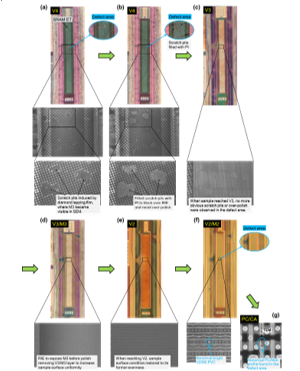 Figure 9. Successful case of sample rescue by using e-beam Pt deposition to repair scratched sample with scratch pits in the ROI. (a) The defect area of the sample got scratch damage when using diamond lapping films to remove top metal layers. (b) To block over-RIE and resist over-polish, e-beam Pt was deposited at the scratch pits to cover the damaged area. (c, d) After the normal RIE and slurry polishing removed V4/M4, the effect of the scratch damage on the V3/M3 layer showed greatly mitigated. (e) At V2 level, the sample had restored to an un-damaged condition, and (f) abnormal bright V2/M2 PVC was observed in the ROI. (g) The defect of abnormal PC/NiSi profile was finally found at the EFI spot location.
With protective Pt filling the scratch pits (Figure 9b), the ROI slowly restored to its former evenness and no more damage feature was seen when the sample reached V2 (Figure 9c-9e), as shown in the successful rescue case. After the M2 was exposed by RIE, optimal surface condition for SEM inspection was obtained and abnormal bright V2/M2 passive voltage contrast (PVC) was observed at the spot location (Figure 9f). The rescue mechanism is illustrated in Figure 6d-6g. The delayering on the sample was then continued from M2 downwards by normal delayering process and finally found the abnormal PC/NiSi at PC/CA level (Figure 9g). TEM images (along PC) are shown in Figure 8. Compared to the reference location, the defect location has abnormal PC/NiSi profile and missing portion of PC which are correlated with the source-drain leakage. PC formation issue in the wafer process is suspected as the root cause. In summary, this case demonstrated simple method of e-beam Pt deposition for tackling the common sample scratching problems induced by diamond film lapping or other incidents in delayering.
3.3. Case 3: Using Controlled Slurry Polishing Combined With Partial RIE to Remove Sample Unevenness and Create Ultra-Large (> 50000 μm2) Inspection Area
The third case is about an ultra-large “snake” metal line ET structure in a 40 nm node device that failed M4 high resistance. To perform PFA on the failed ET, we tried to polish the sample to V4 and identify the physical defect that resulted in the high resistance. The area to be inspected is as big as > 50000 μm2 where a single metal line “snake” runs through the whole ET structure in the wafer scribe line. PVC inspection in SEM is needed to locate the defect position which requires intact connection in the metal line without any damage such as metal bridging or metal broken from the sample preparation. However, when the normal slurry polishing on the sample reached V5, obvious evenness at the ET corners was observed, which would potentially lead to metal smear or break if we continued to polish until V4.
A failed case is shown in Figure 11. The “snake” metal line ET sample had uneven IMD at V5 due to the edge effect, while slurry polish directly proceeded upon full time RIE removing IMD. After M5 was removed, severe M4 unevenness and damage were generated. At the corner areas, the sample was even over-polished to M3. The failure mechanism is shown in Figure 10a-10c, where the IMD unevenness is consider as the root cause. Without intact metal line connection, PVC inspection was not possible. Even if the defect was not damaged, tedious inspection in SEM would be needed to check every piece of metal through the whole large area for the defect.
Figure 10d-10h illustrates how we coped with the issue in the successful case. By smearing the metal lines to form an etch-stop area after the first partial RIE (Figure 10f), the IMD was evened
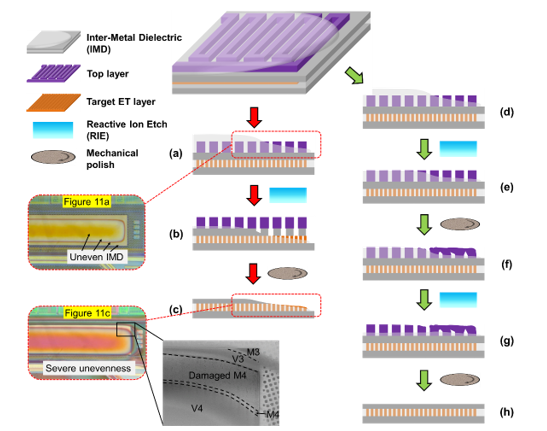 Figure 10: Schematic illustration of the failed case and the successful case of rescuing the uneven samples. (a-c) In the failed case, the edge effect induced unevenness will aggravate along with the slurry polishing, especially for the structure in the scribe lines. (d-g) In the successful case, by smearing the metal lines to form an etch-stop area after the first partial RIE, the unevenness of the IMD will be removed, which will result in an even surface in the next layer. Insets are the OM and SEM images from the failed case.
out by another partial RIE (Figure 10g) to obtain an even surface in the next layer (Figure 10h). The SEM and OM results of the successful rescue case are shown in Figure 13. When the uneven IMD was spotted as circular halo at the ET edge, partial RIE using half of the full RIE time was performed to expose the outer M5 with thinner IMD (Figure 13a). The different division of the RIE time is dependent on different sample conditions including via length and degree of unevenness. More divisions deliver better results in flattening the IMD. In this case, the full RIE time was equally divided into two halves (e.g., if the full time is 20 s, each half will be 10 s). The first partial RIE shrank the IMD halo by around 50% (Figure 13b), which means half of the M5 was exposed. Then we slightly slurry polished the surface until the exposed M5 metal lines collapsed and smeared together. The halo area further shrank smaller because the V5 was polished thinner or nicely fully removed. As a result, three different regions (smeared M5, exposed M5, and un-exposed M5) were generated (Figure 13c). Since the RIE for oxide etching doesn’t chemically react with metal structure, the smeared M5 worked as a mask to block the RIE impact on the IMD4. After the second partial RIE was applied onto the sample, the IMD5 in the areas of exposed M5 and un-exposed M5 was etched down until the same level as that in the smeared M5 area (Figure 13d). The cross-sectional view is illustrated in Figure 10g.
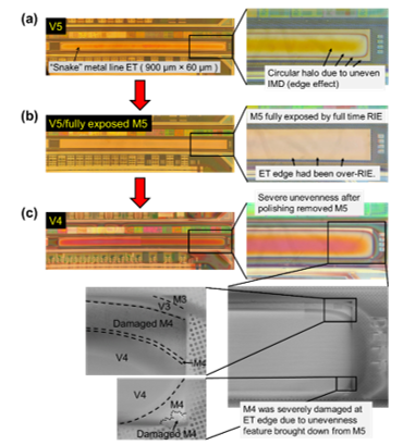 Figure 11: Failed case of delayering ultra-large “snake” metal line ET where (a) the uneven V5/M5 was performed with (b) full time RIE which induced over-exposure of M5 and in turn (c) over-polish on M4.
Finally, after removing M5 by normal slurry polishing, the sample achieved great evenness at V4 across the whole ET structure without any damage to M4. PVC inspection in SEM was then successfully performed and the bright signal was traced along the single ET metal line to quickly locate the defect site where the PVC stopped (Figure 13e). TEM (across the metal lines) analysis on the defect location showed abnormal M4 pattern which was responsible for the high resistance failure, and lithography issue in the wafer process was suspected (Figure 12). In summary, slurry polishing combined with partial RIE is able to generally remove the unevenness induced by edge effect within large areas.
 Figure 12: TEM (across metal line) images of the target location and the reference location. Abnormal M4 pattern was observed at the target location.
Table 1: Summary of PFA techniques for rescuing damaged samples with cracks, scratches, or unevenness in delayering.
| Types | Problems | Solutions |
| Cracks | Polishing difficulty, Edge effect | Balance polishing using dummy; Level the joined samples using diamond lapping films |
| Scratches | Over-RIE, Over-polishing | Deposit Pt on the scratched area to block RIE and resist polishing |
| Unevenness | Edge effect, Limited inspection area | Smear the partial RIE exposed metal, and then even out the IMD by another partial RIE |
4. Conclusion
In this paper, advanced PFA techniques for rescuing damaged samples with cracks, scratches, or unevenness in delayering by finger polishing have been discussed, through three typical FA cases. The first case is on rescuing cracked samples where diamond lapping film and sacrificial dummy were used to cope with the polishing difficulty and the edge effect with the target defect area close to the gaps/crack lines. The second case is about using e-beam Pt deposition to repair the damage in ROI to the scratched samples and restore the sample to its even condition. The third case studied using controlled slurry polishing combined with partial RIE to remove sample unevenness and create ultra-large (> 50000 μm2) inspection areas. These techniques are very useful in helping the FA engineers to tackle accidents, solve problems and deliver high-quality FA results, especially for handling “one of a kind” devices.
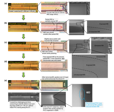 Figure 13: Successful case of sample rescue by using controlled slurry polishing combined with partial RIE to remove sample unevenness and create ultra-large (> 50000 μm2) inspection area in the “snake” metal line ET. (a) A circular halo due to the uneven IMD at the ET edge was observed at V5. (b) M5 was partially exposed by the first partial RIE, and the sample was (b) slightly slurry polished until (c) the exposed M5 was smeared. (d) The second partial RIE was then performed to get rid of the IMD unevenness. (e) After M5 was removed by slurry polishing, the sample achieved great evenness globally through the whole ET structure. With an intact ET metal line, PVC inspection easily located the defect of broken M4.
Conflict of Interest
The authors declare no conflict of interest.
Abbreviations
DOF Depth of Field
EFI Electrical Fault Isolation
ET Electrical Test
FA Failure Analysis
FIB Focused Ion Beam
IMD Inter-Metal Dielectric
Mx Metalx, x is layer number
NA Numerical Aperture
OM Optical Microscope
PFA Physical Failure Analysis
RIE Reactive Ion Etch
ROI Region of Interest
SEM Scanning Electron Microscope
SRAM Static Random Access Memory
TEM Transmission Electron Microscope
Vx Viax, x is layer number
- J. Leo, H. Tan, Y. Z. Ma, S. M. Parab, Y. M. Huang, D. D. Wang, L. Zhu, J. Lam, Z. H. Mai, “Key Issues for Implementing Smart Polishing in Semiconductor Failure Analysis,” Journal of Applied Mathematics and Physics, 5, 1668-1677, 2017, doi:10.4236/jamp.2017.59139.
- M. E. Weldy, L. Serrano, “Increasing Planarity for Failure Analysis Using Blocked Reactive Ion Etching Combined With Planar Polish,” in 2005 International Symposium for Testing and Failure Analysis (ISTFA), 206-208, 2005, doi:10.31399/asm.cp.istfa2005p0206.
- H. Feng, P. K. Tan, H. H. Yap, G. R. Low, R. He, Y. Z. Zhao, B. Liu, M. K. Dawood, J. Zhu, Y. M. Huang, D. D. Wang, H. Tan, J. Lam, Z. H. Mai, “A Sample Preparation Methodology to Reduce Sample Edge Unevenness and Improve Efficiency in Delayering the 20-nm Node IC Chip,” in 2015 IEEE International Symposium on Physical and Failure Analysis of Integrated Circuits (IPFA), 2015, doi:10.1109/IPFA.2015.7224432.
- K. S. Wills, S. Perungulam, “Delayering Techniques: Dry Processes, Wet Chemical Processing, and Parallel Lapping,” Microelectronics Failure Analysis Desk Reference Fifth Edition, 444-463, 2004.
- Y. M. Sub, B. T. H. Yap, F. I. Lee, A. B. Minhar, K. W. Tan, H. J. Looi, T. M. Foo, “A Case of Charging Induced Damage into the Common Metal Interconnect During Chemical Mechanical Polishing,” in 2017 IEEE International Conference on Opto-Electronic Information Processing (ICOIP), 2017, doi:10.1109/OPTIP.2017.8030704.
- K. S. Wills, “Planar Deprocessing of Advanced VLSI Devices,” in 2006 International Symposium for Testing and Failure Analysis (ISTFA), 393-397, 2006, doi:10.31399/asm.cp.istfa2006p0393.
- S. Bott, R. Rzehak, B. Vasilev, P. Kucher, J. W. Bartha, “A CMP Model Including Global Distribution of Pressure,” in 2011 IEEE Transaction on Semiconductor Manufacturing, 304-314, 2011, doi:10.1109/TSM.2011.2107532.
- Y. Y. Meng, L. Zhang, Y. B. Li, W. Zhang, H. F. Zhou, J. X. Fang, “Impact of Bevel Condition on STI CMP Scratch,” in 2020 China Semiconductor Technology International Conference (SCTIC), 2020, doi:10.1109/CSTIC49141.2020.9282450.
- X. Wu, Z. Huang, Y. J. Wan, H. T. Liu, X. Chen, “A Novel Force-Controlled Spherical Polishing Tool Combined With Self-Rotation and Co-Rotation Motion,” in 2020 IEEE Access, 108191-108200, 2020, doi:10.1109/access.2020.2997968.
- A. Wieters, P. Thieme, “Wafer Edge / Bevel Treatment of Device Wafers by Means of CMP,” in IEEE 2007 International Conference on Planarization / CMP Technology (ICPT), 2007.
- T. Moor, E. Malyanker, E. R. Moyal, “Single Die ‘Hand-Free’ Layer-by-Layer Mechanical Deprocessing for Failure Analysis or Reverse Engineering,” in 2008 International Symposium for Testing and Failure Analysis (ISTFA), 2008, doi:10.31399/asm.cp.istfa2008p0363.
- H. H. Yap, P. K. Tan, G. R. Low, M. K. Dawood, H. Feng, Y. Z. Zhao, R. He, H. Tan, J. Zhu, B. H. Liu, Y. M. Huang, D. D. Wang, J. Lam, Z. H. Mai, “Top-down Delayering to Expose Large Inspection Area on Die Side-edge with Platinum (Pt) Deposition Technique,” Microelectronics Reliability, 55, 1611-1616, 2006, doi:10.1016/j.microrel.2015.06.037.
- H. G. Ong, C. L. Gan, “Alternative Lapping Method to Reduce Edge Rounding Effect,” in 2012 International Symposium for Testing and Failure Analysis (ISTFA), 462-464, 2012.
- K. P. Park, H. S. Kim, O. Chang, H. S. Jeong, “Effects of Pad Properties on Material Removal in Chemical Mechanical Polishing,” Journal of Materials Processing Technology, 187-188, 73-76, 2007, doi:10.1016/j.jmatprotec.2006.11.216.
- L. X. Wu, C. F. Yan, “Effects of Polishing Parameters on Evolution of Different Wafer Patterns During Cu CMP,” in 2015 IEEE Transaction on Semiconductor Manufacturing, 106-116, 2015, doi:10.1109/TSM.2014.2387211.
- D. Lim, H. Kim, B. Jang, H. Cho, J. Kim, H. Hwang, “A Novel Pad Conditioner and Pad Roughness Effects on Tungsten CMP,” in IEEE 2014 International Conference on Planarization / CMP Technology (ICPT), 352-355, 2014, doi:10.1109/ICPT.2014.7017318.
- C. Wang, P. Sherman, A. Chandra, D. Dornfeld, “Pad Surface Roughness and Slurry Particle Size Distribution Effects on Material Removal Rate in Chemical Mechanical Planarization,” CIRP Annals-Manufacturing Technology, 54, 309-312, 2005, doi:10.1016/S0007-8506(07)60110-3.
- T. F. Zeng, T. Sun, “Size Effect of Nanoparticles in Chemical Mechanical Polishing – A Transient Model,” in 2005 IEEE Transaction on Semiconductor Manufacturing, 655-663, 2005, doi:10.1109/TSM.2005.858508.
- C. J. Evans, E. Paul, D. Dornfeld, D. A. Lucca, G. Byrne, M. Tricard, F. Klocke, O. Dambon, B. A. Mullany, “Material Removal Mechanisms in Lapping and Polishing,” CIRP Annals, 52, 611-633, 2003, doi:10.1016/S0007-8506(07)60207-8.
- L. Shan, C. H. Zhou, S. Danyluk, “Mechanical Interactions and Their Effects on Chemical Mechanical Polishing,” in 2001 IEEE Transaction on Semiconductor Manufacturing, 207-213, 2001, doi:10.1109/66.939815.
- “Microscopy Basics: Depth of Field and Depth of Focus”, Nikon, https://www.microscopyu.com/microscopy-basics/depth-of-field-and-depth-of-focus.