Designs of Frequency Reconfigurable Planar Bow-tie Antenna Integrated with PIN, varactor diodes and Parasitic Elements

Adv. Sci. Technol. Eng. Syst. J. 6(4), 320–326 (2021);
 DOI: 10.25046/aj060435
This paper presents the designs and the simulations of proposed structures of electronically frequency reconfigurable planar bow-tie antenna. In the first part, a modified wide band self-complementary bow-tie antenna is designed and implemented. In the second part, varactor and PIN diodes are integrated in top side to adjust electronically the modified structure of bow-tie antenna over multi-band frequency. By adjusting PIN diode between the two states and by tuning the varactor diode inside these two states; the proposed antenna demonstrates two different operational frequencies. In ON state, the antenna covers a narrow frequency bands and in OFF state the antenna demonstrates a wide-band operational frequency. Furthermore, a new structure of reconfigurable antenna implemented with PIN diode and two hexagonal parasitic elements is developed to realize a multi-band operational frequency band and to cover GPS and GMS bands. Simulated results show a return loss less than -10dB with a gain varied between 0.5 and 3.5dB.
1. Introduction
In the modern communication system, frequency reconfigurable antenna has been achieved an important extension as for as adjusted operated band and low cost.
Indeed, various structures designs are implemented to improve configurability. In [1], mechanical control method is employed to creat a different operated frequency band. Nevertheless, this methode proposals several problems in comparison with the electronical control method which can achieve an important exactitude and a very fast speed. Electronic control method is more commonly used [2]-[4] based to RF switches such as PIN diodes, MEMS or varactor diodes. Those RF switches can adjust the effective length of the antenna which can tune the frequency band of the antenna when the control bias is varied.
A frequency reconfigurable microstrip slot antenna is designed and implemented in [5]. The proposed antenna structure can switch between six different operation frequency bands using five RF PIN diodes. Those switches are integrated in the slot of the antenna to adjust the effective length of the slot. Measured results demonstrate a return loss less than -10dB at the different frequency bands, a gain equal to 4dB and a bidirectional radiation patterns.
In [6], A compact PIFA antenna is realized to cover UHF DVB-H frequency band. The antenna is implemented using three PIN and a varactor diodes. Three metallic strips are integrated between the radiation element and the ground plane via PIN diodes when the largest metallic strips is directly soldered to the ground plane. Moreover, a lateral short circuit is related to the ground plane via varactor. Simulation results demonstrate four configurations with the appeared of different frequency bands in each configuration.
Varactor and PIN RF switches were employed to adjust the frequency of reconfigurable bow-tie antenna operate over (3-6GHz). Measured results show a reflexion coefficient less than -10dB over the different wide operational frequency bands and a stable radiation patterns with a gain varied between 3.21dB and 5.42 dB [7].
In [8], authors proposed a new configuration which consist to integrate PIN diodes over the bow-tie arms to switch the antenna between Bluetooth, Wimax and Wlan bands. Measurements demonstrated an important results.
In this paper, we propose different structures of frequency reconfigurable antenna which can switch between wideband and narrow band operational frequency. The proposed structures of reconfigurable antenna have been demonstrated a multi-bands operation in two states with acceptable results.
In the second section, we present the implementation, the simulation and the measurements of the proposed structure of SCBT antenna.
In section 3, a PIN and a varactor diodes are added in the top side of the SCBT antenna to realize a frequency reconfigurable antenna which is switched between a simple frequency band and two dual frequency bands in ON state and a wide-band operational frequency in OFF state.
Then, a proposed structure based on PIN diode and two hexagonal parasitic elements is developed. The two parasitic elements are integrated in the front and in the back side of the antenna structure to produce a new frequency bands over (1.49-1.7GHz) in ON state and over (1.77-1.85GHz) in OFF state.
2. Implementation of SCBT antenna
A wide-band performance is required in the modern wireless communication systems. To obtain this goal, several wideband antennas are implemented in the literature such as Bow-tie antenna which demonstrates an important performances over a wideband frequency [9]-[11].
In this section, a proposed structure of the SCBT antenna is designed and realized using FR4 substrate.
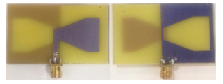 Figure 1: Prototype of proposed bow-tie antenna
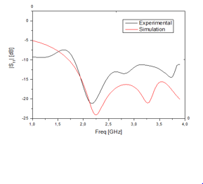 Figure 2: Bow-tie antenna Measurement and simulation
This proposed structure presents good performances such as wideband operation and simple implementation and feeding [12]. The antenna dimensions are calculated using the formulas in [12] and they are optimized via CST: L=54.4mm; W=41.07mm; Wt =2.4mm; Lt =23mm; Wp =25.6mm; Lp =21.5mm; Ls =28.6mm; Wr =0.6mm. Therefore, the size of the modified antenna structure is (50×40 mm2). The top and bottom views of the structure design are shown in figure 1.
The simulation results are checked through experimental measures figure 2. Simulation return loss is validated with the experimental result and it shows a reflection coefficient less than -10 dB over (2-4GHz). The simulation results of gain patterns are presented in figure.3.
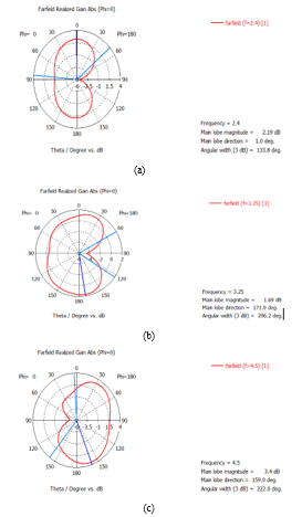 Figure 3: Gain patterns at f= 2.4, 3.25 and 4.5GHz
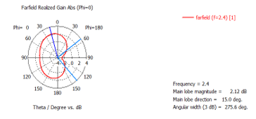
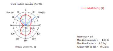
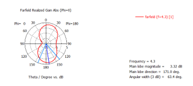
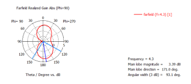
Three frequencies are chosen to determine the generated gain inside the operational band. Therefore, simulation results of modified SCBT antenna demonstrated a gain equal to 2.19dB, 1.69dB, 3.4dB at 2.4GHz, 3.25GHz and 4.5GHz respectively, with a bidirectional radiation patterns in E plane.
3. Frequency reconfigurable SCBT antenna using PIN and varactor diodes
3.1. Design and Simulation
Varactor and PIN diodes are implemented in the top side of the antenna structure to switch the antenna among different operational frequency bands figure 4. Therefore, the BAR 64-05w PIN diode is used to control the antenna between the two states. When the ON state is selected, the antenna can achieve a narrow operational frequency band. Otherwise, when the OFF state is selected we can show a wideband operational frequency.
The varactor diode used is MA46585 with a capacitance varied between (0.14 pF to 2.2 pF). By adjusting the reverse bias of the varactor diode between (0V-30V), the varactor capacitances values are improved and the antenna can select the looked-for band frequency. The varactor is modeled in the simulation as a capacitor in series with a forward resistance and inductor. Antenna size is equal to (50×40) mm2.
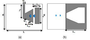 Figure 4: Proposed frequency reconfigurable bow-tie antenna implemented with PIN and varactor diodes: (a) Front view (b) Back view
When the applied Bias control is (V=0.82V), PIN diode is modeled by the resistance R=2.7Ω. Thus, when the diode is tuned ON and by adjusting the varactor capacitances value, different narrow frequency bands are appeared. when the value of the varactor diode capacitance is equal to 0.14pf or 0.19pf, we can show a dual band operational frequency. However, when the capacitance value is fixed to 0.75 pf the antenna is pointed to a simple narrow frequency band.
Otherwise, when the no bias voltage is applied (V=0); the diode is modeled by the capacitor C= 0.22pf. Indeed, three wide bands are obtained when the varactor capacitances value is equal to 0.14pf, 0.19pf and 0.75pf.
The determined simulation results in the two states are presented in figure 5.
When the diode is switched ON and the varactor capacitance is adjusted to 0.75pf, simulation results show a reflection coefficient less than -10dB over a narrow frequency band (1.83-2GHz). Then, a dual band frequency is shown while the varactor capacitance is tuned to 0.19pf. The first band is varied among (2.2-2.5GHz) and the second band occupies the frequencies (3.5-4.2GHz), reflection coefficient in resonance frequencies is equal to -35dB and -18dB at 2.2GHz and 3.6GHz respectively. Two others dual band are achieved when the varactor capacitance is tuned to 0.14pf, the first band is varied between (2.2-2.5GHz) and the second band occupies the frequencies (4.1-4.4GHz). Return loss in resonance frequencies is equal to -60dB and -24dB at 2.1GHz and 4.3GHz respectively. However, when the PIN diode is switched OFF and the varactor capacitance is adjusted to 0.75pf, the reflection coefficient is less than -10dB over (3.5-5GHz). When the varactor capacitance is tuned to 0.19pf the antenna shows a wideband operation with a reflection coefficient less than -10dB. The frequency band is varied among (2.1-5GHz). When the varactor capacitance is adjusted to 0.14pf, the antenna presents wideband frequency operation over (2.1-4.4GHz). Figure 6 proves the gain patterns in ON state with varactor capacitances 0.75 pf, 0.19 pf and 0.14 pf and the gain patterns in OFF state with varactor capacitances 0.75 pf, 0.19 pf and 0.14 pf is illustrated in figure 7.
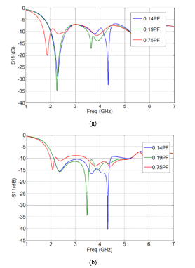 Figure 5: Return loss of reconfigurable antenna with different capacities values: (a) in ON state, (b) in OFF states
 E Plane
 H Plane
(a)
 E Plane
 H Plane
 E Plane
(b)
 E Plane
 H Plane
 E Plane
 H Plane
(c)
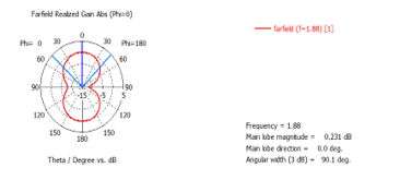
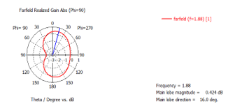
Figure 6: Gain patterns in ON state (a) C=0.75pf, (b) C=0.19pf, (d) C=0.14pf.
 E Plane
 H Plane
(a)
 E Plane
 H Plane
(b)
 (c)
(c)
E Plane
 H Plane
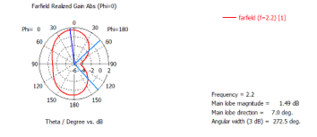
Figure 7: Gain patterns in OFF state (a) C=0.75pf, (b) C=0.19pf and (c) C=0.14pf
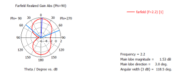
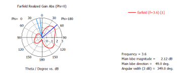
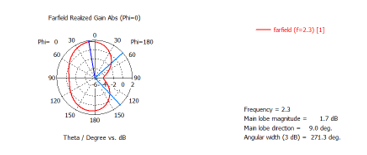
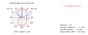
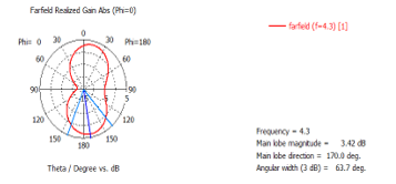
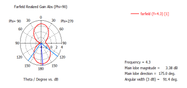
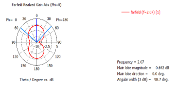
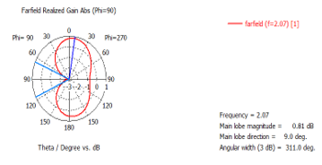
Gain patterns results in ON state present a gain equal to 0.231dB at 1.88GHz when the varactor capacitance is on 0.75pf, a gain varied between 1dB and 2.8dB when varactor capacitance is on 0.19pf and a gain around 3.42dB when varactor capacitance is on 0.14pf. In OFF state, the gain is varied between 0.64dB and 3.32 dB over the three wideband frequency. Consequently, bidirectional pattern has been shown and circular polarization has been produced.
4. Frequency reconfigurable SCBT antenna using PIN diode and two parasitic elements
4.1. Design and Simulation
In this section, the idea is to integrate two hexagonal parasitic elements in the front and in the back antenna structure which provide a new operational frequency bands. Using this proposed configuration, GPS and GMS band have been covered. Antenna structure is shown in figure.8.
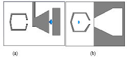 Figure 8: Proposed reconfigurable bow-tie antenna integrated with PIN diode and two parasitic elements: (a) Top view (b) Bottom view
We can show Multi-bands frequency operation when the two states are commuted. In figure 9, the reflection coefficients of the proposed antenna are illustrated.
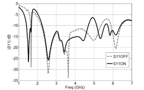 Figure 9: Reflection coefficient results
Simulation results demonstrate two different states with multi-bands operation frequency. The simulated reflection coefficients are less than -10dB at all frequency bands of the two states. In ON state, the improved frequency bands are (1.5-1.75GHz), (2.3-4.61GHz) and (5.15-5.95GHz). At the resonance frequencies 1.58GHz, 3.51GHz and 5.71GHz, the reflection coefficients are -25dB -22,5dB, -34dB respectively. When the OFF state is selected, the obtained frequency bands are (1.77-1.85GHz), (2.24-5.1GHz) and (5.8-6.5GHz) and the reflection coefficients at the resonances frequencies ,1.81 GHz, 2.41 GHz and 5.81 GHz, are -28dB, -32dB and -15dB.
Simulated gain patterns in the two states are presented in figures 10-11.
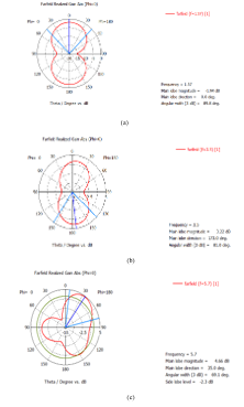 Figure 10: Gain patterns in ON state at 1.58GHz (a), (b) 3.51GHz, (c) 5.71GHz
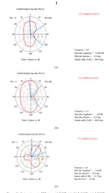 Figure 11: Gain patterns in OFF state at 1.81GHz (a), (b) 2.41GHz, (c) 5.81GHz
Simulated gain patterns demonstrate the disparity of gain between 2.2dB and 4.7dB and a gain equal to -1.9dB at f=1.58GHz in ON state. when the OFF state is selected, generated gain is restricted to 3.55dB at all operational frequencies and a bidirectional pattern has been shown. Consequently, the proposed antenna provides a circular polarization.
5. Comparison study
Using the parasitic elements, we can show two states with a multi-band operational frequency; the structure is characterized by the simple design and a low control voltage (0v-3v). However, antenna structure using PIN and varactor diodes demonstrates six states which show a simple narrow band, dual-band and wide band operational frequency. The structure requires a two bias voltage with control voltage of (0v- 3v and 15v).
Table 1: Results Table
| STATES | Varactor | Parasitic elements | ||
| C1=0.14pf | C2=0.19pf | C3=0.75pf | ||
| ON: | Dual-band
[2.2-2.5 GHz] [4.1-4.4 GHz] |
Dual-band
[2.2-2.5 GHz] [3.5-4.2 GHz] |
[1.83-2 GHz] | [1.49-1.7GHz]
[2.29-4.6GHz] [5.1-5.9GHz] |
| OFF: | [2.1-4.4GHz] | [2.1-5GHz] | [3.5-5GHz] | [1.77-1.85GHz]
[2.24-5.1GHz] [5.8-6.5GHz] |
| Reference | Type of switches | Number of switches | Antenna size (mm2) | Number of achieved
Bands |
Bandwidth of Each Subband |
| [5] | RF PIN | 5 | 50×46 | 6 narrow bands | ͌500MHz |
| [13] | RF PIN
|
5 | 50×100 | 5 narrow bands | ͌300MHz |
| [14] | PIN &varactor | 2 | 30×70 | 6 narrow bands | 100MHz<BW<700MHz |
|
Proposed |
PIN &varactor | 2 | 50×40 | 3narrow bands
& 3wide bands |
200MHz<BW<3GHz |
| PIN&
Parasiticelements |
1 | 50×40 | 2 states with multi-bands in each state | 200MHz<BW<3GHz |
6. Conclusion
In this paper, two structures of electronically reconfigurable antenna are designed and simulated. First proposed structure is developed based on PIN and varactor diodes. Thus, three frequency bands are appeared in each state with a good return loss and acceptable gain (1 to 3.5dB). Using this configuration, antenna can commute between a narrow band and a wide band operational frequency. Proposed antenna size is (50×40mm). The second structure of reconfigurable antenna is based on simple PIN diode and two hexagonal parasitical elements implemented in the top and the bottom side of the substrate. The proposed structure can cover GMS and GPS band and it can realize a multi-band operational frequency in each state. Simulation results show an important performance corresponding to the gain and reflection coefficient. Structure size is (50×40mm).
- Y. Tawk and C.G Christodoulou, “A new reconfigurable antenna design for cognitive radio,” IEEE Antenna wireless prog.lett., 8, 1378-1381, 2009, DOI: 10.1109/LAWP.2009.2039461.
- A. C. K. Mak, C. R. Rowell, R. D. Murch and C. L. Mak, “Reconfigurable Multiband Antenna Designs for Wireless Communication Devices, ” IEEE Transactions on Antennas and Propagation, 55(7), 1919-1928, 2007, doi: 10.1109/TAP.2007.895634.
- D.Peroulis, K. Sarabandi, and L. P. B. Katehi, “Design of reconfigurable slot antennas,” IEEE Trans. Antennas Propag., 53(2), 645–654, 2005, doi: 10.1109/TAP.2004.841339.
- W.H. Weedon, W.J. Payne and G. M. Rebeiz, “MEMS Switched reconfigurable antenna,” In Procceeding of the IEEE International Symposuim on Antenna And Propagation, 3, 654-657, 2001, doi: 10.1109/APS.2001.960181.
- Huda A. Majid, M. Kamal A. Rahim, M. Rijal Hamid and M. F. Ismail, “A Compact Frequency-Reconfigurable Narrowband Microstrip Slot Antenna,” IEEE Antennas And Wireless Propagation Letters, 11, 616 – 619, 2012, doi: 10.1109/LAWP.2012.2202869 .
- F. Canneva. F. Ferrero, J.M. Ribero, R. Staraj, “Reconfigurable miniature antenna for DVB-H standard,” IEEE Antennas and Propagation Society International Symposium,” 2010, doi: 10.1109/APS.2010.5561955.
- Tong Li, Huiquing Zhai, Long Li and changhong Liang, “Frequency –Reconfigurable Bow-tie antenna with a wide tuning Range,” IEEE Antennas and Wireless Propagation Letters, 13, 1549 – 1552, 2014, doi: 10.1109/LAWP.2014.2344676.
- Tong Li, Huiquing Zhai, Long Li and changhong Liang, “Frequency-Reconfigurable Bow-Tie antenna for Bluetooth, Wimax and Wlan application,” IEEE Antennas and Wireless Propagation Letters, 14, 171 – 174 , 2015, DOI: 10.1109/LAWP.2014.2359199.
- Abdelnasser A. Eldek, Atef Z. Elsherbeni, and Charles E. Smith, “Wideband Microstrip-fed Printed Bow-tie Antenna For Phased Array Systems,” Microwave And Optical Technology Letters, 43, 123–126, 2004, doi: 10.1002/mop.20396.
- Tutku Karacolak and Erdem Topsakal , “A Double-Sided Rounded Bow-Tie Antenna (DSRBA) for UWB Communication,” IEEE Antennas And Wireless Propagation Letters, 5, 446 – 449, 2006, doi: 10.1109/LAWP.2006.885013.
- Ray, K. P., “Design Aspects of Printed Monopole Antennas for Ultra-Wide Band Applications,” International Journal of Antenna and Propagation, 1-8, 2008, doi: 10.1155/2008/713858.
- Khalil H. Sayidmarie, Yasser A. Fadhel, “A Planar Self-Complementary Bow-Tie Antenna for UWB Applications ,” Progress In Electromagnetics ResearchC, 35, 253-267, 2013, doi:10.2528/PIERC12103109
- Yoon-Seon Choi , Ji-Hun Hong , Jong-Myung Woo, “Electrically and Frequency-Tunable Printed Inverted-F Antenna with a Perturbed Parasitic Element,” Journal Of Electromagnetic Engineering And Science, 20(3), 164-168, 2020, doi:10.26866/jees.2020.20.3.164.
- Jong-Hyuk Lim, Gyu-Tae Back, Young-Il Ko, Chang-Wook Song, and Tae-Yeoul Yun, “A Reconfigurable PIFA Using a Switchable PIN-Diodeand a Fine-Tuning Varactor for USPCS/WCDMAM-WiMAX/WLAN,” IEEE Transactions On Antennas And Propagation, 58(7), 2404 – 2411, 2010, doi: 10.1109/TAP.2010.2048849.
No related articles were found.