Development of Miniaturized Monolithic Isolated Gate Driver

Adv. Sci. Technol. Eng. Syst. J. 6(5), 177–184 (2021);
 DOI: 10.25046/aj060520
Gate driver has been applied in many ways, exemplified by that, by using the DC-isolated and AC-pass characteristics of gate driver’s primary and secondary sides, the problem of floating endpoint in semiconductor power switch can be solved. However, the conventional design of isolated gate driver provides circuit voltage blocking by optically coupled components. Due to the need for optoelectronic conversion, it requires III-VI semiconductor process and non-standard CMOS process, and the cost is always high. Therefore, in order to better solve the above mentioned problem, an electronic isolated gate driver is proposed. It employs an on-chip transformer to provide voltage isolation between the primary and secondary sides of the circuit, and converts the control signal in the circuit into a high-frequency modulated signal, which in the secondary side is then demodulated by the rectifier through the on-chip transformer to produce the original control signal. The miniaturized isolated gate driver proposed herein adopts TSMC T25HVG2 process and uses an on-chip transformer design in lieu of an optically coupled components. As the amplitude shift keying, on-chip transformer, full-wave quadruple rectifier and data buffer amplifier involved in this design are all integrated on the same chip, the integration can be improved. The size can be smaller than the generally separating electronic isolated gate driver, with the interference from external noise being reduced. In addition, the proposed gate driver generates large signals, in terms of chip layout, therefore, the circuit is put inside the on-chip transformer, which can further save area.
1. Introduction
Conventional galvanic isolated gate drivers use optically coupled components for a high degree of voltage isolation. Due to the need for optoelectronic conversion, it requires III-VI semiconductor process and non-standard CMOS process, and the cost is always high. In desirous of solving these problems, MOSFET electronic isolated gate driver has been studied as a new direction. It couples the energy to the secondary side of the transformer by the transformer’s resonant coupling method in lieu of the optical coupling driver. Since the isolation is realized by optical and electrical energy conversion, many of the shortcomings in the traditional design can be improved, such as the larger size and higher process cost in the past.
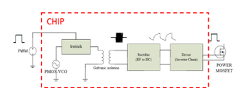 Figure 1: System concept of proposed isolated gate driver.
This paper is an extension of work originally presented in the 2nd IEEE Eurasia Conference on IOT, Communication and Engineering 2020[1]. The proposed system concept in which is shown in Figure 1. The circuit is mainly composed of a VCO, a mixing circuit (Switch), an on-chip transformer, a quadruple rectifier and a data buffer amplifier. We input a PWM-controlled signal to the chip, and then the ~1 GHz oscillation signal and the PWM signal are modulated by ASK (amplitude shift keying) at the switch, and then the modulated signal is brought to the secondary side by the on-chip transformer; the quadruple rectifier then further amplifies the small signal and rectify the DC voltage of the process to provide enough driving voltage for the data buffer amplifier to generate the PWM signal, and that’s the expected result.
The circuit proposed is integrated on a single chip, so the size is much smaller than the separated design [2, 3]; besides, according to the simulation, if a PWM control signal of 100- kHz 50% duty circle is given at the primary side’s input end, we hope that after the voltage isolation, the output can remain the same. However, on account of the transmission delay caused by the rise time and fall time, the output PWM control signal will be slightly degraded as the simulation shows that the duty circle of the output PWM control signal is 48.4%, a difference of 1.6%; the difference between the rise time and fall time is only 0.2 μs. In the next section, we introduce the architecture of the chip, and discuss the detailed circuit design and the model of the on-load transformer in detail in the implementation section. Finally, we present the results of different process variations under Post-Simulation in Full-chip Simulation, all of which are in line with the expected specifications.
2. Chip architecture
The system block diagram and schematic diagram proposed in this article are shown in Figure 2 and Figure 3, respectively. Its primary side is composed of a current mirror with a current controller and a PMOS VCO. The input PWM signal and the 1GHz signal provided by the oscillator, after modulation, are transmitted to the secondary side through the on-chip transformer. The full-wave quadruple rectifier can further amplify and demodulate the modulated signal into a DC voltage. However, the potential and ripple of the rectified DC voltage is not suitable for being directly used as a gate drive signal, and the data buffer amplifier can improve this problem by further pulling the voltage to 5 V and greatly improving the ripple, so as to increase its driving force.
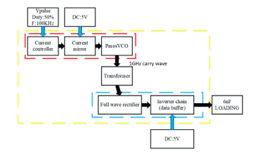 Figure 2: The system block diagram of the proposed design.
On and off of the switch can be controlled by putting a PWM control signal on the primary side. Once the switch is on, the current will increase. At this point, the large current causes the VCO to generate a larger amplitude oscillation signal. That is, as the current becomes larger or smaller, the PMOS VCO generates two signals with different amplitudes. The above phenomenon can be interpreted as that, the carrier wave generated by the PMOS VCO and the PWM signal are subjected to an ASK modulation action, and then the modulation signal is transmitted to the secondary side through the on-chip transformer. However, since this signal voltage level is not high enough to drive the data buffer amplifier, the full-wave rectifier (voltage multiplier) will increase the voltage level and rectify the RF signal to a DC voltage. Finally, the data buffer amplifier further enhances the driving capability. In addition, the data buffer amplifier converts the ASK signal into a PWM gate signal to drive the subsequent semiconductor power switch.
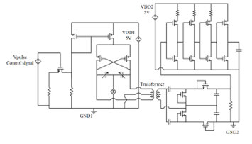 Figure 3: The schematic diagram of the proposed isolated gate driver.
There are two types of transformers for on-chip transformer design: stack transformer or tapped transformer [1, 4]. It provides galvanic isolation in the circuit proposed in this article. The stack transformer performs better in coupling, but its isolation is limited by process as the distance between the metal layers is fixed. In other words, although the coupling degree of the tapped transformer is less than that of the stack transformer, the distance between the two inductors is longer than that of the stack transformer. The transformer is more flexible. The transformer applied in this paper is a stack transformer which features higher coupling as mentioned above.
3. Circuit implementation
3.1. Current Mirror with Current Controller
The current controller, shown in Figure 4, consists of two resistors and a switch. The switch is controlled by a PWM control signal generated by a signal generator outside the chip. When the switch is on, the two resistors become parallel, which makes the impedance smaller and current higher (Figure 5). The lower part of Figure 5 is the input current of Figure 4 current mirror, and the upper part of Figure 5 is the output current after magnification of 3 times by the Figure 4 current mirror. This design serves the purpose of performing ASK modulation of the PWM signal and the oscillation signal. Another reason for this design is that if the OOK modulation is achieved by simply turning off the oscillator instead of generating oscillation signals of different amplitudes, it takes more time for the system to enter the steady-state mode, which causes even longer transmission delay. Therefore, in order to achieve ASK modulation, the oscillation signal needs to be decreased so that it cannot drive the data buffer amplifier instead of directly closing the entire system.
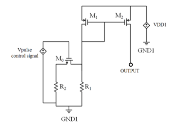 Figure 4: The schematic of current mirror and current controller
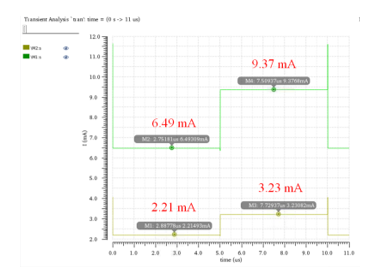 Figure 5: The output current of the current controller and the output current after going through the current mirror.
A current mirror is employed to increase the current, and the result is shown in Figure 5. The lower curve is the current value of current controller side and the upper curve is the current value that follows into VCO. When the voltage control signal is low, the current values of the current control and VCO are 2.21 mA and 6.49 mA, respectively. When the voltage control signal is high, the current values of the current control and VCO are 3.23 mA and 9.73 mA, respectively. The current mirror magnifies the current to a set magnification, such as (1). Since L1 = L2 and W2 = 3W1 in this design, the magnification should be 3 times the current in Figure 5, and the result is obtained. M is Magnification of current mirror.
M = (W2 · L1) / (W1 · L2) (1)
3.2. PMOS Voltage Control Oscillator
T The main function of the VCO is to change the capacitance value by adjusting VBIAS [4-6], thereby generating different oscillation frequencies. As this LC resonant circuit is composed of an inductance with fixed inductance value and a variable capacitance, this study can therefore increase the exhaustion region in the diode by enhancing the reverse bias voltage of the VCD. Therefore, when the reverse bias voltage becomes larger, the distance between the two metals in the VCD increases, the capacitance value decreases, and the resonance frequency of the LC circuit reduces. In addition, the PMOS VCO design proposed in this paper must achieve the ASK modulation effect with a current mirror with a current controller, that is, the PWM signal and the oscillation signal generated by the PMOS VCO need to be modulated.
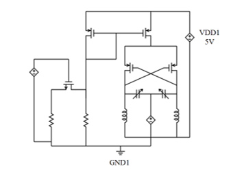 Figure 6: The circuit schematic of the PMOS VCO.
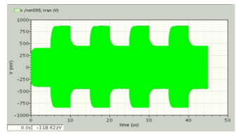 Figure 7: The output signal of the PMOS VCO with the current control voltage low and high.
As shown in Figure 7, the current controller and current mirror make the VCO generate low and high currents, which further makes the PMOS VCO generate two RF signals with different amplitudes. Generally, it takes longer to reach a stable state after the VCO oscillation stops. Therefore, it needs to make the small oscillation signal keep oscillating, and the signal must be small enough so as not to affect the components in the design proposed herein.
3.3. Stack transformer
The stack transformer [1, 4, 7], shown in Figure 8, is chosen because of its higher theoretical coupling, which means that, compared with the tapped transformer [8, 9], the stack transformer can transmit signal to the secondary side more effectively. However, the stack transformer still has shortcomings. The distance between the two inductors is limited by the process, that is to say, the distance between each layer is fixed, which means that the isolation is limited. A tapped transformer, however, uses a same layer (metal in the top), so the distance between the metals is more flexible despite the lower degree of coupling. The results are shown in Figure 9 and 10, indicating that the inductance value is about 3.57 nH, the quality factor is about 6.94, and the coupling coefficient is about 0.917 at 1 GHz.
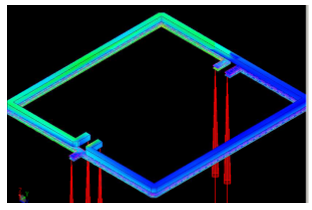 Figure 8: 3D graph of the stack transformer.
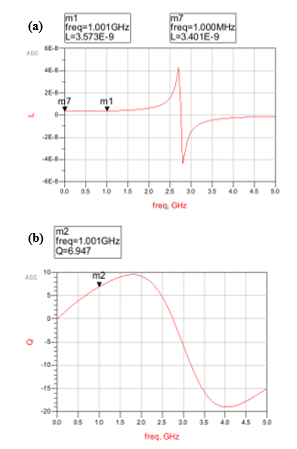 Figure 9: (a) The inductance of transformer and (b) Quality factor in the primary side.
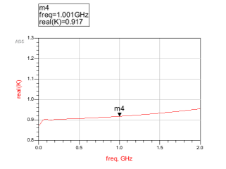 Figure 10: Coupling coefficient of the proposed transformer.
Figure 11 shows the modeling of the on-chip transformer proposed in this paper [10]. R11 and R21 are the impedance of the transformer itself at low frequency. The values of L10 and L20 in Figure 11 are from the model of the ADS momentum transformer. L11, L21 , R10, R20 are the inductance and impedance generated by the proximity effect and skin effect [11,12] when the two on-chip inductors are at high frequencies. Cox and Rsub are the parasitic resistance and capacitance between the metal layer and the substrate, and Cps is the coupling capacitance between the two inductors.
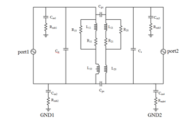 Figure 11: Modeling of the on-chip transformer.
In the circuit, L10 and L20 can be obtained by (2), and the result is shown in Figure 9. L10 and L20 are the inductance values in the circuit at low frequency, so we can get this data in Figure 9 (a). R11 and R21 are also the impedance of the circuit at low frequency, so its parameters can be obtained in smith and z_parameter by the same way. Cp and Cs are the parasitic capacitances in the inductance, which can be reversely obtained according to its natural vibration frequency, such as (3) (4). The natural vibration frequencies of the primary side and the secondary side are represented by freqp and freqs respectively [13].
L10 = imag( Z11 ) / ( 2 · pi · freq ) (2)
freqp = 1 / [2 · pi · sqrt(L10 · Cp)] (3)
freqs = 1 / [2 · pi · sqrt(L10 · Cp)] (4)
As the chip itself is a 1:1 symmetrical architecture, Rsub1 = Rsub2 = Rsub3 = Rsub4, and Cox1 = Cox2 = Cox3 = Cox4. we can see the comparison between the simulation and the optimized modeling from Figure12. In Figure 12, curves of S(1,1), S(2,2) and S(1,2) are from ADS momentum simulation in Figure 8, and curves of modeling2..S(1,1), modeling2..S(2,2) and modeling2..S(1,2) are from optimized modeling in Figure 11. Coupling coefficient K and quality factor Q can be obtained from (5) (6). The difference between the results of ADS momentum simulation and optimized modeling simulation is shown in Table 1.
K = sqrt(imag(Z12) · imag(Z21)) / sqrt(imag(Z11) · imag(Z22)) (5)
Q = imag( Z11 ) / real( Z11 ) (6)
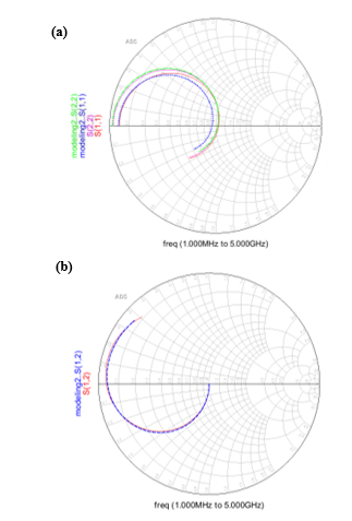 Figure 12: Comparison of the results between ADS momentum (Figure 8) and modeling (Figure 11) (a) S11 and S22 (b) S12 results
Table 1: Comparison of s parameter simulation and modeling simulation
| ADS momentum | Optimized Modeling | |
| R20 | 0.78 ohm | 0.65 ohm |
| L20 | 3.16 nH | 3.51 nH |
| R10 | 2.36 ohm | 2.17 ohm |
| L10 | 3.40 nH | 3.33 nH |
| freqp | 2.75 GHz | 3.05 GHz |
| freqs | 2.75 GHz | 3.05 GHz |
| K | 0.91 | 0.93 |
| Q | 6.94 | 8.43 |
3.4. Full Wave Rectifier (Voltage Multiplier)
Since the RF signal received from the transformer output is low, the full-wave rectifier rectifies the RF signal to a DC voltage and multiplies the signal, making it has a greater ability to drive the data buffer amplifier. Figure 13 is the circuit schematic of the full-wave rectifier [14] proposed in this paper.
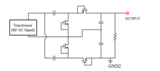 Figure 13: Proposed full-wave rectifier.
The traditional voltage multiplier is a diode voltage doubler in cascaded capacitor, where the voltage doubler uses voltage multipliers to connect N stages. If the threshold voltage is regarded as zero, it can theoretically reach N times of magnification. However, Zener diode threshold voltage and low threshold NMOS cannot be regarded as zero. In the formula (7), VIN is the amplitude of the RF oscillation signal, VT is the threshold voltage, and N is the series of voltage multiplier in cascaded capacitor.
VOUT = 2N · (VIN – VT) (7)
However, conventional diode multipliers come with the disadvantages of high output impedance, large DC output ripple, and low conversion efficiency. Therefore, in this study, the proposed design replaces the Zener diode with a low threshold voltage NMOS (Figure 13).
3.5. Data buffer
The data buffer amplifier consists of four inverters connected in series. The basis of the data buffer is to effectively enhance the driving capability of the gate signals [15]. In addition, it also reduces the transmission delay of the signal in inverters. Figure 14 shows the relationship between the delay time and the different stages of the inverter chain. N is the design time, f is the ratio of Cin to Cout, and tp is the transmission delay of signal through the data buffer amplifier. As N increases, tp can be reduced. This design serves the purpose of effectively reducing the ratio of electrical output capacitance to gate capacitance in each stage, and of gradually increasing the current size of each stage, so that it can shorten the rise and fall times by connecting a multi-stage inverter and thus reduce the transmission delay, which is better than the original small capacitor charging a large one. However, this stage connection has its limits as too many stages make the output of the signal generate excess delay, and the size is not easy to control. The advantage of the four-stage architecture adopted in this paper is that the phase of the output control signal is the same as that of the primary side’s PWM control signal, and the transmission delay can be minimized to avoid too many long stage connections.
Since the capacitance ratio of each stage in the four-stage architecture is three times larger than that of the previous stage, the gate capacitance (Cin) can be changed by application of CMOS technology, the width and length of MOSFET. In other words, since the inverter chain proposed in this paper consists of four inverters, the width of the next MOSFET stage needs to be modified so that it is three times larger than that of the previous MOSFET.
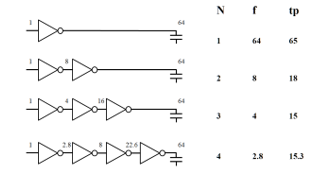 Figure 14: Signal delay time with different stage inverter.
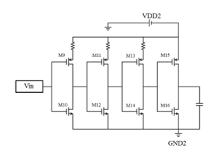 Figure 15: Proposed data buffer.
In the design, DC voltage cannot be used directly as a gate control signal for gate driver because of its large ripple and long rise and fall times. Therefore, the data buffer amplifier is an important element to improve the drawback by enhancing the drive capability. In the proposed design (Figure 15), the data buffer amplifier consists of four inverters and three resistors. Since the rectified DC voltage is not sufficient to drive the data buffer, the resistors are used to lower the threshold of the driving voltage. The four-stage data buffer can also amplify the input current by 64 magnitudes, which allows the circuit to generate enough current to drive the potential larger power MOSFET. In addition, the inverter chain eliminates ripples and also reduces fall and rise times.
4. All chip simulation
This monolithic isolated gate driver proposed in this paper is designed and manufactured with TSMC 250nm HV COMS technology and 5 V transistors. The on-chip transformer, with area 1.000 mm × 1.125 mm, provides galvanic isolation between the primary and secondary sides. The control signal sets a 100- kHz 50% duty cycle 5-V PWM signal for the current controller to switch the current value. The VCO generates 1-GHz oscillation signals of different amplitudes due to the different magnitudes of current from the current mirror and the current controller. The results are shown in Figure 16.
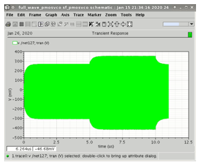 Figure 16: The oscillation signal of the PMOS VCO.
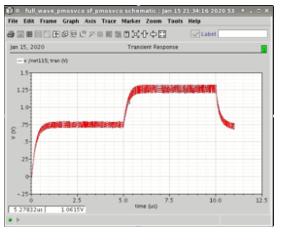 Figure 17: The output voltage of the full wave rectifier.
The signal generated by VCO is not high enough to drive the data buffer amplifier, so the full-wave rectifier amplifies the voltage and rectifies the RF signal to DC voltage, as shown in Figure 17. The driving threshold voltage of the data buffer amplifier is shown in Figure 18, and the threshold voltage of the four-stage chain is around 1V. When the driving voltage is higher than 1V, the rectified signal can trig the inverter chain. When the driving voltage is lower than 1V, it cannot trig. The results are shown in Figure 18(a). Figure 18(b) shows the result when resistors are not added to the data buffer amplifier to reduce its threshold drive voltage, its original voltage is about 2.5 V. The threshold drive voltage that requires more voltage multipliers to be larger leads to extra energy loss and chip size increase due to the too many components.
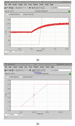 Figure 18: (a) The threshold of the data buffer is ~1V. (b) the threshold voltage in data buffer without resister is ~2.5 V
In the final design, after the signal passes through the whole system, the duty cycle of the PWM signal with 50% duty cycle is kept at 48.4% and the rise and fall times are kept below 10% of the cycle (rise and fall times are about 0.2 μs, and the cycle time at 100 kHz is 10 μs). The results are shown in Figure 19.
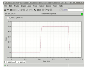 Figure 19: The output of the data buffer.
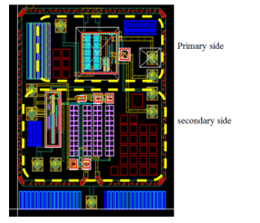 Figure 20: Chip layout
Table 2: In case of different corners, the expected result and the simulation result of changing the control DC bias of the variable vessel
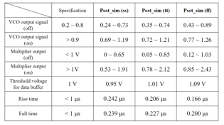 Table 2 shows the specifications and simulation results of the circuit proposed in this paper. The output voltages of the VCO and multiplier vary depending on the control voltage given to the varactor diode. It needs attention in the circuit, because in design, VCO must generate two different voltages, and after the two voltages are rectified by the voltage quadrupler, one of the rectified DC voltages needs to be able to drive the data buffer amplifier, while the other rectified DC voltage cannot drive the data buffer amplifier, so as to ensure that these two voltages can control the first-stage inverter of the data buffer amplifier, making the circuit generate PWM control signals. Assuming that this condition cannot be guaranteed to be established, it may cause the data buffer amplifier to become routinely open or closed, which leads to the failure to achieve our expected results. In addition, the varactor also makes it difficult for the VCO to start up as shown in Table 2. As to the output signal of VCO and the voltage amplifier, the result also increases as the control DC bias of the varactor increases, which means that if insufficient or too much control DC bias is given, it may cause the first-stage structure of the inverter chain to be routinely open and closed, thus making the circuit lose its intended function. Figure 20 shows the layout of the chip to be delisted. This gate driver generates large signals, so the layout of this chip puts the circuit inside the on-chip transformer to save more area.
5. Conclusion
Traditional isolated gate drivers generally adopt optically coupled driver components to achieve high isolation, so they require III-VI semiconductor process and non-standard CMOS process, making the cost even higher. In order to solve this problem, electronic isolated gate drivers are gradually attracting more attention. On-chip transformers can reduce the energy loss caused by the optical coupling components, but a separate architecture is still used in many designs – devices with different functions are designed on different chips, which leads to other problems, such as larger size, and poor treatment of external noise. Therefore, the problem of high cost remains unsolved in such designs. The architecture proposed in this paper is to integrate the whole oscillator, transformer, full-wave multiplier and rectified DC signal processing system on one chip, so as to reach optimization in both integration and size.
On the primary side, the signal generator provides the chip with a 100 kHz PWM switching signal with a 50% duty cycle, which is then modulated by a ~1 GHz carrier wave generated by a VCO. After passing through a full-wave rectifier and a data buffer amplifier, it retains a 48.4% duty cycle and a 5-V output signal. All devices are integrated in a single chip. This will reduce the system dimension and enhance the system integration significantly.
Conflict of Interest
The authors declare no conflict of interest.
Acknowledgment
This research is supported by the Ministry of Science and Technology, Taiwan, R.O.C. under Grant no. MOST 107-2221-E-018-002- and MOST 109-2221-E-018-007-. We are thankful to the National Chip Implementation Center (CIC) for making its EDA tools and technology available, and the National Center for High-performance Computing (NCHC) for the use of its computer time and facilities.
- H.Y. Kuo, J.J.Lin, “Implementation of Miniaturized Monolithic Isolated Gate Driver,” in 2nd IEEE Eurasia Conference on IOT, Communication and Engineering 2020, ECICE 2020, 129–132, 2020, doi:10.1109/ECICE50847.2020.9301940.
- S. Nagai, Y.Yamada, N.Negoro, H.Handa, M.Hiraiwa, N.Otsuka, D.Ueda, “A 3-phase AC-AC matrix converter GaN chipset with drive-by-microwave technology,” IEEE Journal of the Electron Devices Society, 3(1), 7–14, 2015, doi:10.1109/JEDS.2014.2364307.
- C. Liu, D.Mandal, Z.Yao, M.Sun, J.Todsen, B.Johnson, S.Kiaei, B.Bakkaloglu, “A 50-V Isolation, 100-MHz, 50-mW Single-Chip Junction Isolated DC-DC Converter with Self-Tuned Maximum Power Transfer Frequency,” IEEE Transactions on Circuits and Systems II: Express Briefs, 66(6), 1003–1007, 2019, doi:10.1109/TCSII.2018.2869074.
- J. Lin, K.C.Lin, “A monolithic isolated gate driver with on-chip transformer and a Voltage Level Shifter,” in 2017 IEEE 3rd International Future Energy Electronics Conference and ECCE Asia, IFEEC – ECCE Asia 2017, 1256–1259, 2017, doi:10.1109/IFEEC.2017.7992223.
- M. DaTsai, Y.H.Cho, H.Wang, “A 5-GHz low phase noise differential colpitts CMOS VCO,” IEEE Microwave and Wireless Components Letters, 15(5), 327–329, 2005, doi:10.1109/LMWC.2005.847696.
- X. Wang, B.Bakkaloglu, “Systematic design of supply regulated LC-tank voltage-controlled oscillators,” IEEE Transactions on Circuits and Systems I: Regular Papers, 55(7), 1834–1844, 2008, doi:10.1109/TCSI.2008.918004.
- A.Ghadiri, K.Moez, “Bandwidth enhancement of on-chip transformers using negative capacitance,” IEEE Transactions on Circuits and Systems II: Express Briefs, 59(10), 648–652, 2012, doi:10.1109/TCSII.2012.2213360.
- H.M.Hsu, C.W.Tseng, K.Y.Chan, “Characterization of on-chip transformer using microwave technique,” IEEE Transactions on Electron Devices, 55(3), 833–837, 2008, doi:10.1109/TED.2007.914841.
- R. Wu, N.Liao, X.Fang, S.Member, “A Silicon-Embedded Transformer for High-Efficiency, High-Isolation, and Low-Frequency On-Chip Power Transfer,” 62(1), 220–223, 2015. doi:10.1109/TC.2015.2517635.
- Q. El-Gharniti, E.Kerhervé, J.B.Bégueret, “Modeling and characterization of on-chip transformers for silicon RFIC,” IEEE Transactions on Microwave Theory and Techniques, 55(4), 607–615, 2007, doi:10.1109/TMTT.2007.893647.
- J.Kang, L.Sun, J.Wen, M.Zhao, “An equivalent lumped-circuit model for on-chip symmetric intertwined transformer,” in ASICON 2009 – Proceedings 2009 8th IEEE International Conference on ASIC, IEEE: 674–677, 2009, doi:10.1109/ASICON.2009.5351336.
- J. Liu, L.Sun, Z.Yu, “An accurate compact model for on-chip vertically coiled transformers,” IEEE Electron Device Letters, 34(4), 484–486, 2013, doi:10.1109/LED.2013.2247559.
- H. Liao, C.Wang, “A New Approach to Parameter Extraction for On-Chip Symmetric Transformers,” in 2009 IEEE International Symposium on Radio-Frequency Integration Technology, RFIT 2009, IEEE: 257–260, 2009.
- S. Iqbal, “A hybrid symmetrical voltage multiplier,” IEEE Transactions on Power Electronics, 29(1), 6–12, 2014, doi:10.1109/TPEL.2013.2251474.
- X.J. Wang, T.Kwasniewski, “Propagation Delay-Based Expression of Power Supply-Induced Jitter Sensitivity for CMOS Buffer Chain,” IEEE Transactions on Electromagnetic Compatibility, 58(2), 627–630, 2016, doi:10.1109/TEMC.2016.2517635.