Low-Power Primary Cell with Water-Based Electrolyte for Powering of Wireless Sensors

Adv. Sci. Technol. Eng. Syst. J. 6(5), 267–272 (2021);
 DOI: 10.25046/aj060529
In this work we discuss a special technique for powering of sensor systems, based on a low-power primary cell consisting of two electrodes, made from different metals, with water (lake, rain or tap water) used as an electrolyte. Once placed into an aqueous solution, the primary cell generates a small electric current, which may be utilized for powering of sensor systems. The generated electrical energy is fed into an energy storage (capacitor). After transformation of the voltage by a step-up converter, it is used for supplying the electrical sensor circuit. The expected output power of the developed circuit is 10-15 mA by 2 V output voltage during 0.2-0.5 second. The improved voltage converter topology with implemented maximal power point techniques allows significant reduction of the energy storage’s size in the second revision of the circuit and thus reduction of the resulting size of the board. The implemented sensor board with discussed powering technique, assembled in Paderborn University was already tested in different practical scenarios.
1. Introduction
This paper is an extension of work originally presented in 2020 IEEE Sensors [1]. Energy harvesting technologies are often used for powering of wireless sensors, especially for industrial monitoring applications [2]. Powering techniques like photovoltaic and thermoelectric generators are widely presented on the market, but there is always a need for new ideas for energy powering techniques [3]. The Sensor Technology Group at Paderborn University is directly developing the power supply system for wireless sensors based on a galvanic cell used for generation of small electrical currents with a water-based electrolyte (lake, rain or tap water) [1, 4].
The wireless sensors powered by the developed electrochemical cell can be used e.g., for construction monitoring and detection of water leakages in roofs or wall structures of industrial and private buildings. Such sensors integrated in building structures can get activated by contact with water, caused by a water leakage. This water serves as an electrolyte for the galvanic cell, which provides the electrical energy for the sensor electronics. The main advantage of this approach is a long sensor lifetime in the not activated state, longer than most batteries’ durations that are currently available on the market (usually up to 10 years).
2. Implementation of a galvanic cell
The implemented galvanic cell with two metal electrodes mounted on the non-conductive substrate (composite epoxy material) is depicted in Figure 1, left. To perform the measurements, the developed cell is placed inside the vessel with tap water serving as an electrolyte (Figure 1, right).
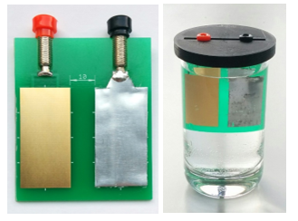 Figure 1: The implemented setup of a galvanic cell with two metal electrodes (left), and galvanic cell placed in water, serving as electrolyte (right)
The difference of electric potential between two electrodes results from the standard potential of the chosen electrode metals [5-7].
During the experimental measurements, multiple combinations of electrode materials have been compared and tested. The practically established parameters of the galvanic cells (short-circuit current and open-circuit voltage) are depicted in Figure 2.
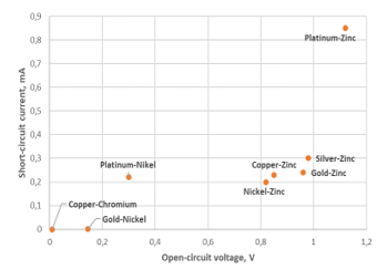 Figure 2: Established parameters for different metals, used for galvanic cell electrodes with electrode areas of 8 cm2 (4 x 2 cm), in tap water [1]
Table 1 shows the standard electrochemical potentials of commonly used electrode materials [5].
Table 1: Standard electrochemical potential of metals commonly used as electrode materials
| Electrode material | Reaction pair | Standard potential, V |
| Gold | Au3+ + 3e– | 1.5 |
| Gold | Au2+ + 2e– | 1.69 |
| Platinum | Pt2+ + 2e– | 1.2 |
| Silver | Ag+ + e– | 0.80 |
| Copper | Cu+ + e– | 0.52 |
| Zinc | Zn2+ + 2e– | -0.76 |
Although the pair platinum and zinc results in the highest value of output power, a combination of zinc and gold metals has been selected for the developed galvanic cell [8], because gold finish is a standard coating technique in the production of printed circuit boards (PCB). A gold layer of 100-200 nm is typically used to protect the contact pads of the PCB against corrosion and simplifies the soldering process [9]. An adequate gold thickness allows the stable operation of the implemented cell, although, any defect in the gold layer (like fracture or porosity) reduces the generated power by reducing the open-circuit voltage.
Figure 3 shows the established performance of the implemented cell with gold and zinc electrodes of 8 cm2 area (4 x 2 cm), loaded to a capacitance of 50 mF. The distance between the electrodes was 10 mm. The calculated energy saved in the capacitor achieved 9,8 mJ after 5 minutes and about 11 mJ in 10 minutes.
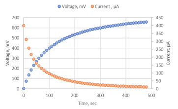 Figure 3: Current and voltage curves charging a capacitance of 50 mF [1]
Figure 4 depicts the load curve of the developed galvanic cell. The established open-circuit voltage is around 700 mV, the corresponding maximum power point (MPP) is about 250 mV. The calculated generated power achieves up to 44 µW, if the galvanic cell operates close to the MPP voltage.
The performance of the tested galvanic cell working on the capacitive load (shown in Figure 3) could be improved by connecting a voltage converter working with the established maximum power point between the output of the galvanic cell and charged capacitance. This design of the voltage converter will be discussed in detail in chapter 4.
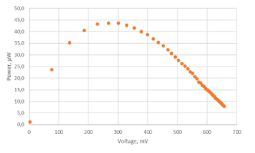 Figure 4: The load curve of the galvanic cell consisting of Au and Zn.
3. Sensor board design
The selected combination of gold and zinc electrodes connected by water ensures an open circuit voltage of about 700 mV. This voltage is lower than the operating voltage of typical electronic circuits (from 1.8 V to 2.0 V for common low-voltage microchips). The maximal output current of the developed galvanic cell is between 100 and 200 µA (short-circuit current), this is much lower than the typical current consumption of wireless transmitter ICs (10 to 15 mA). Therefore, a step-up voltage converter circuit was implemented to boost the output cell voltage. The harvested energy has to be integrated and must be stored temporarily in an energy storage circuit, e.g., a capacitor or super capacitor, until the energy amount is high enough to power the sensor circuit for the required time (0.2 to 0.5 seconds).
The first revision of the developed sensor board uses a super capacitor as an energy storage component. It is connected between the output of the galvanic cell and the input of the voltage boost circuit. The block diagram of this first revision is shown in Figure 5. After charging the super capacitor up to 700 mV (threshold voltage), the chosen step-up converter is starting up. It boosts up performs the voltage to 2.0 V to supply the electrical circuit of the sensor board. After complete discharging of the super capacitor, the charging cycle will be repeated. The low-voltage synchronous boost converter, TPS61201 from Texas Instruments [10], was implemented in the first revision of the developed sensor board.
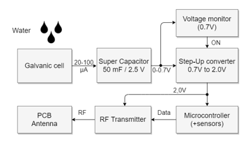 Figure 5: Block diagram of the developed circuit board with energy storage connected to the input of the voltage converter
The required capacitance of the super capacitor is between 20 and 50 mF, which is enough to deliver the estimated current of 10-15 mA over a time interval of 0.2 to 0.5 seconds. For the super capacitor, a model produced by AVX company with a capacity of 50 mF was used in the voltage converter circuit [11]. To supervise the charging process of the super capacitor, a discrete low-voltage detector by RICOH with 0.7 V threshold voltage is used [12].
The first revision of the sensor PCB (with a size of 27 mm x 100 mm) is depict in Figure 6. Two metal electrodes, each at a size of 8 cm2, are located on the bottom side of the board. The electronic components are placed on the upper side of the PCB. The electrical contact between the gold coated positive electrode and the electrical circuit is performed by a through-hole connection (the black point at the top right corner of the left electrode). The negative (zinc) electrode is cut out of a zinc plate, the mechanical and electrical connections of the zinc electrode to the upper side of the PCB is realized by two flaps, inserted into board openings and connected to the contact pads on the top side. The openings are sealed with silicone to prevent the electrical contact of the sensor circuit with the electrolyte.
On the top side of the developed sensor board the supercapacitor is located on the left, the voltage converter and transmitter circuit in the middle of the board, and the RF antenna on the right side. A complete sealing of the electrical circuit (the complete top side of the board) could also be implemented for practical applications to protect the circuit from the moisture and dust.
The total component cost for the first revision of the developed sensor PCB is about 9.0 € (calculated for 1000 pieces).
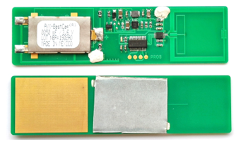 Figure 6: Design of the first revision of the sensor board (top and bottom side)
4. Optimized sensor board design
The minimal size of the first revision of the developed board is defined by the size of the super capacitor (energy storage), which occupies about 30% of the board area. The new improved topology of the power supply circuit which is currently implemented, uses the maximum power point (MPP) tracking technique. It allows an operation of the galvanic cell close to the point of maximal efficiency. In this topology the energy storage is placed between the output of the step-up converter and the sensor electronics. Here the storage capacitor can be charged to a higher voltage level (3.3 V instead of 0.7 V) giving the possibility to save considerably more electrical energy, thus reducing the required capacitance. This allows less expensive alternatives to the supercapacitor, like tantalum capacitors. By using the new topology, the sensor PCB area may be reduced by about 30%. The block diagram of the second revision of the sensor board with implemented MPP tracking is depict in Figure 7.
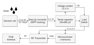 Figure 7: Block diagram of the sensor board with energy storage at the output of the voltage converter and implemented MPP tracking
Using the selected ADP5091 voltage converter with implemented MPP tracking by Analog Devices [13] increases the output power of the galvanic cell and significantly reduces the charging time (from 8-10 minutes to 3-4 minutes). Further optimisation of the electrode sizes and relation between gold and zinc area help to reduce the total size of the sensor board from 100 mm x 27 mm to 75 mm x 27 mm (reduction by 25%). The component costs in this version were also reduced by about 30%. The total costs for the second revision of the sensor PCB are about 6.5 € (from 1000 pieces).
The second revision of the sensor board is shown in Figure 8. The tantalum capacitors for storing the generated electrical energy (two orange blocks on the top side of the PCB) occupy only a small part of the sensor board area. The voltage converter is located on the left and the RF antenna with the transmitter circuit on the right side of the sensor PCB.
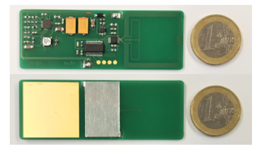 Figure 8: Design of the second revision of the sensor board (top and bottom side)
Both, gold and zinc electrodes are placed on the bottom side of the board. The optimized relation between gold and zinc areas (up to 1:2) allows to significantly reduce the electrode area. The size of the gold electrode was reduced from 25 x 32 mm to 25 x 25 mm (reduction by 22%) and the size of the zinc electrode was reduced from 25 x 32 mm to 25 x 14 mm (reduction by 56%).
5. Wireless data transmission
The amount of collected electrical energy should be high enough to perform the initialization of the EFM8 low-power MCU by Silicon Labs [14], the measurement tasks, and additionally the wireless transmission of the data packages via Si4012 RF transmitter [15]. The power consumption of the RF transmitter circuit is most significant compared to other parts of the circuit. Additionally, the current consumption changes very quickly, depending of the data transmission cycle. Knowing the current profile of the RF transmitter helps to design the power supply circuit and to calculate the required amount of electrical energy for the sensor operation. The measured real-time current consumption of the transmitter circuit is shown in Figure 9.
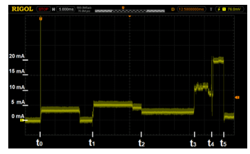 Figure 9: Current consumption of the RF transmitter with the time scale according to the Table 2
This measurement was realized by measuring the voltage drop over a shunt resistor, placed in the supply line of the transmitter circuit.
The important time intervals of the data transmission are shown in Table 2. The calculated energy value is 0.7 mJ for start-up of the transmitter module and the first transmitted data packet, and 0.3 mJ for following data packets. Between transmission of data packets, the transmitter IC goes in a power down mode, reducing the current consumption down to few microamperes.
Table 2: Measured Current consumption of RF transmitter
| Time interval | Task | Current, mA | Power, mW |
| t0 – t1 | Power-on | 3.5 | 7.0 |
| t1 – t2 | Initialize | 5.0 | 10.0 |
| t2 – t3 | Compose data package | 4.0 | 8.0 |
| t3 – t4 | Initialize transmission | 10.0 | 20.0 |
| t4 – t5 | Data transmission | 19.0 | 38.0 |
Sending of multiple sequential packages reduces the probability of a data loss (e.g., by interfering of a single packet with electromagnetic noise spikes). However, the multiple data packets increase the energy budget of the sensor system. In the first revision of the sensor board, the number of repetitions counts was 4 to 6 data packages, depending on the charging state of the super capacitor.
The implemented randomized time intervals between the individual packages, shown in Figure 10, should additionally increase the safety of the data transmission.
In the second revision of the sensor board a number of 2 to 3 transmitted packets was implemented and successfully tested, which helps to reduce the required energy budget of the sensor circuit almost by 50% (considering the power consumption of the MCU, not affected by reducing the number of transmitted packets).
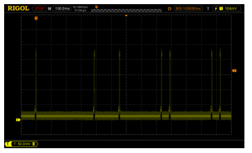 Figure 10: Multiple data packets with randomized time intervals
To keep the time of a single data transmission as short as possible, the length of the data package was also decreased to a minimum: the package consists out of two bytes preamble, four bytes of payload and additional two bytes for the control sum (CRC-16), leading to a total length of the data package of only 8 bytes (Table 3). Since the implemented sensors operate as simple water detectors with transmitting only their unique ID number, the payload bytes are currently holding the four bytes of the sensor ID. For other sensor implementations for measuring and transmitting of additional parameters the packet length needs to be adjust correspondingly.
Table 3: Transmitted data packet
| Byte 1 | Byte 2 | Byte 3 | Byte 4 | Byte 5 | Byte 6 | Byte 7 | Byte 8 |
| Preamble | Preamble | ID-1 | ID-2 | ID-3 | ID-4 | CRC-16 | CRC-16 |
6. Receiver board
To receive and evaluate the sensor data, a receiver board based on the Si4355 866 MHz RF receiver module by Silicon Labs [16] was developed. The block diagram of the receiver board is shown in Figure 11.
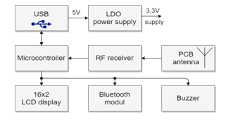 Figure 11: Block diagram of the receiver board [1]
The received data packets are decoded by the RF receiver module, the payload data are processed by the MCU and send via USB interface to the external system. The received data packets are also shown on the built-in LCD display, additionally the buzzer tone signalizes the receipt of a new packet. The received packets can also be transmitted wirelessly via Bluetooth interface to a tablet or a mobile phone. The developed receiver board is powered via USB interface from the host device.
The photo of the developed receiver board is depicted in Figure 12. The USB interface is located on the left side of the board, the receiver IC and the RF antenna are placed on the right side of the main PCB, separated from the main part of the electrical circuit and having their own ground area. The pin-header on the top side of the PCB is used to connect the external LCD display, in the middle the FT232RL USB to UART interface by FTDI Chip [17] and the power supply circuit are located.
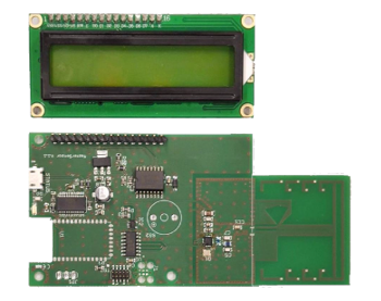 Figure 12: Receiver board with external LCD display module
The receiver board is controlled by an ATtiny1614 microcontroller by Microchip [18]. To address all the implemented interfaces an additional 16-bit port expander IC is used [19]. The Bluetooth module [20] is placed on the bottom left side of the PCB (not assembled in the current revision of the board).
The connected and powered receiver board is shown in Figure 13. The LCD display is mounted above the receiver circuit, covering most electronic components. The connected USB cable also powers the receiver board from the host PC. The LCD display shows the programmed firmware revision in the first line and the last received data packet (sensor ID number) in the second line.
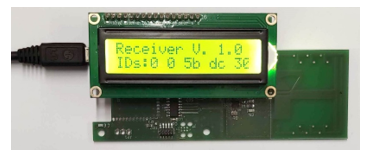 Figure 13: Assembled and powered receiver board showing the last received data packet on the LCD display
The measured transmission range was up to 150 meters outdoors and 30 to 40 meters indoors. According to the orientation of transmitter and receiver antennas, the transmission range may deviate by 20-30%.
A bidirectional communication between sensors and receiver board has not been implemented in the current revision of the sensor system, caused by the small energy budget and limited by the size of the sensor board.
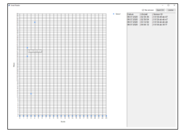 Figure 14: Developed sensor mapping software for time-based representation of activated sensors
7. Developed PC software
For some practical applications (e.g., construction monitoring and detection of water leakages), a graphical depiction of sensor mapping with a time-based representation of activated sensors may help to establish the starting point for water leakages inside the monitored building. An example of the developed software with graphical representation of activated sensors is shown in Figure 14.
On the left side of the display the last activated sensors are shown with the blue points. The list of activated sensors including the sensor ID with a corresponding time stamp is shown on the right side of the window. The sensor mapping feature with graphical representation of the physical sensor placement inside the monitored area is not implemented in the current revision of the software; it will be developed in the next revision.
8. Conclusions
The developed system for powering of wireless sensor systems uses a build-in galvanic cell. It may be used in different scenarios, where the use of conventional batteries is not desired or not possible. Another advantage compared to battery powered systems is a significantly longer storage time of the galvanic cell.
After initiating the galvanic cell, that means both cell electrodes get in contact with water, the lifetime of the cell will be limited by corrosion of the negative (zinc) electrode. The confirmed lifetime can take some days to some weeks, depending on the application and the type of used electrolyte. The confirmed lifetime makes possible the implementation of different scenarios, like water detectors, one-way sensors for environment parameter control etc.
The first revision of the sensor PCB with a size of 27 x 100 mm assembled at Paderborn University was already tested in different practical scenarios.
The second revision of the energy supply circuit with implemented MPP tracking has a higher efficiency in combination with a smaller PCB size of 27 x 75 mm. It also allows a reduction of the resulting board dimension by 26%. The total components cost in the second revision were reduced by about 30%.
The energy supply circuit in combination with the galvanic cell generates enough energy for sending data packages every 3-5 minutes. By increasing the size of the electrodes, more complex sensor systems with higher energy budgets can be implemented.
The developed receiver board receives and evaluates the transmitted sensor data. The received data packages are also shown on the built-in LCD display and forwarded via USB interface to the host-PC. They can be transmitted wirelessly via Bluetooth interface to a tablet or a mobile phone.
The corresponding PC software with the time-based representation of activated sensors in a graphical form including the list of activated sensors with corresponding time stamp was also developed.
9. Outlook
Further optimisation of the sensor board could focus on the transmitter circuit including the transmitter antenna, which currently occupies about 30% of the board size. Another antenna topology with a smaller size should be investigated and implemented.
Furthermore, the operation characteristics of the developed cell under varying environment conditions (humidity and temperature) should be investigated.
Additionally, methods to increase the generated output power could be explored, e. g. by coating the electrodes with material influencing the conductivity of the water and therefore increasing the output power (e.g., natrium chloride, or citron acid).
The developed PC software can be improved by some additional features like a sensor mapping tool with a graphical representation of the physical sensor placement inside the monitored area. The option of combining the registered sensors to different sensor groups (e. g. for monitoring of different objects) is also possible.
- D. Petrov, U. Hilleringmann, “Water-based primary cell for powering of wireless sensors”, IEEE Sensors 2020
- G. Tuna, V.C. Gungor, „Energy harvesting and battery technologies for powering wireless sensor networks”, Industrial Wireless Sensor Networks, 2016
- F. Mazunga, A Nechibvute, “Ultra-low power techniques in energy harvesting wireless sensor networks: Recent advances and issues”, Scientific African, Volume 11, 2021
- H. F. Rezaei, A. Kruger and C. Just, “An energy harvesting scheme for underwater sensor applications”, Electro/Information Technology (EIT), 2012 IEEE International Conference on. IEEE, 2012
- R. A. Huggins, Advanced batteries: materials science aspects, Springer, 2009
- J. Marple, Primary Battery Design, Encyclopedia of Applied Electrochemistry. Springer, New York, 2014
- D. Linden, “Handbook of batteries”, Fuel and energy abstracts, 1995
- K. B. Lee, L.Lin, “Electrolyte-based on-demand and disposable microbattery”, Journal of Microelectromechanical Systems, 12, 1-8, 2003.
- Multi-CB, Printed circuit board surface finish, [Online]. Available:
https://www.multi-circuit-boards.eu/en/pcb-design-aid/surface/surfaces.html. Accessed on: Apr. 25, 2021. - Texas Instruments, TPS6120x Low Input Voltage Synchronous Boost Converter, [Online]. Available: http://www.ti.com/lit/ds/symlink/ tps61200.pdf. Accessed on: Apr. 25, 2021.
- AVX, SuperCapacitors, BZ Series, [Online]. Available: http://www.avx.com/products/supercapacitors/bestcapreg-bz-series. Accessed on: Apr. 25, 2021.
- RICOH, Low Voltage Detector, [Online]. Available: https://www.mouser.de/datasheet/2/792/r3116-ea-1770467.pdf. Accessed on: Apr. 25, 2021.
- Analog Devices, Ultralow Power Energy Harvester PMU with MPPT and Charge Management, [Online]. Available: https://www.analog.com/en/products/adp5091.html. Accessed on: Apr. 25, 2021.
- Silicon Labs, Ultra Low Power Microcontrollers, [Online]. Available: https://www.silabs.com/mcu/8-bit/efm8-sleepy-bee/device.efm8sb10f8g-qfn20. Accessed on: Apr. 25, 2021.
- Silicon Labs, Crystal-less RF Transmitter, [Online]. Available: https://www.silabs.com/documents/public/data-sheets/Si4012.pdf. Accessed on: Apr. 25, 2021.
- Silicon Labs, FSK Sub-GHz receiver, [Online]. Available: https://www.silabs.com/documents/public/data-sheets/Si4355.pdf. Accessed on: Apr. 25, 2021.
- FTDI Chip, USB Full Speed to Serial UART IC, [Online]. Available: https://ftdichip.com/products/ft232rl. Accessed on: Apr. 25, 2021
- Microchip, 8-bit AVR microcontroller, [Online]. Available: https://www.microchip.com/wwwproducts/en/ATTINY1614. Accessed on: Apr. 25, 2021
- NXP Semiconductors, Remote 8-bit I/O expander [Online]. Available: https://www.nxp.com/part/PCF8574T#/. Accessed on: Apr. 25, 2021
- DSD TECH Bluetooth 4.0 module, [Online]. Available: http://www.dsdtech-global.com/2017/08/hm-10.html. Accessed on: Apr. 25, 2021