Improving of Heat Spreading in a SiC Propulsion Inverter using Graphene Assembled Films
 , Torbjörn Thiringer 2, Yasin Sharifi 3, Marco Majid Kabiri Samani 4
Adv. Sci. Technol. Eng. Syst. J. 6(6), 98–111 (2021);
 DOI: 10.25046/aj060614
The focus of this work is first to establish the effect of the chip temperature and thermal feedback on the determination of the power loss in a three-phase propulsion inverter, then to demonstrate the possibility of achieving an improved heat spreading through the different layers inside a SiC power module by using graphene assembled films in the packaging of the power module. The power loss analysis has been carried out for two Silicon Carbide (SiC) modules in a vehicle inverter, incorporating the MOSFET’s reverse conduction as well as including the impact of blanking time on the inverter on-state losses. This data for calculating the losses is determined at an operating situation below the field weakening speed with a high torque for a permanent magnet synchronous machine (PMSM). The operating point is found to be the worst operating condition point when looking at the power loss point. First, it can be noted that not accounting for the thermal feedback, the power loss is considerably underrated, i.e.,11-15% on the on-state converter. Following, the analysis of utilizing the graphene layer in the SiC module reveals a reduction of 10°C per SiC chips in the junction temperature of the SiC MOSFET is achievable. The reduction is calculated based on an applied power loss per SiC chips in steady-state simulation. Furthermore, up to 15°C decrease in the transient computation over the Worldwide Harmonized Light Vehicles Test Cycle (WLTC) per SiC chip is noticed. Moreover, a reduction up to 50% for the junction to case thermal resistance (Rth,JC) is observed by adding the graphene layer in the power module.
1. Introduction
Increasing the efficiency of vehicle inverters for electrified powertrains is becoming a significant demand [1]. Improved Wide Band Gap silicon carbide (SiC) MOSFETs are promising replacements of the standard silicon insulated gate bipolar transistors (Si IGBTs) in EV applications [2–4]. This is a result of lower switching losses due to quicker switching transitions, as well as good thermal properties in the SiC MOSFETs, superior to those of Si IGBTs. Moreover, lower the on-state losses can be reduced through the utilization of the MOSFET’s ability to also conduct current in the opposite direction [5, 6]. Therefore, improving the efficiency of the propulsion inverter utilizing SiC MOSFETs, can lead to reduced losses in the powertrain, which results in a higher power density, to some extent also through the reduction of cooling significantly threaten the performance and lifetime of the semiconductor chips and dies in high power applications. A possibility to tackle this issue is enhanced thermal conduction in various directions inside the power module with effective cooling of the semiconductor chips. Integrating heat spreading materials with excellent mechanical and thermal properties for the power electronics packaging can efficiently move the heat away from the power devices, resulting in a lower operating temperature of the system [7].
Compared to metal materials, nano-scaled carbon materials, in especial, graphene, have a thermal conductivity up to 5300 W/m.K [8], ten times higher than that of the metals [7, 9] as well as an amazing lightweight property, 2.2 g/cm3 and good stability [7], [10, 11]. Particularly, compared with the single layer graphene, there is the incentive in fabricating graphene assembled films (GFs) as new heat spreading materials [12–15] due to their promising electrical and thermal properties. Consequently, research community as well as manufacturers have put intensive efforts into the research on new high-thermally conducting materials like graphene as an effective heat spreader and these efforts have been reported in literature [16–21]. In [22–24] research on the usage of graphene as a spreader of heat in power modules packaging have been conducted. Further interesting research are in [25–27] and a procedure for studying graphene transistors using standard TCAD tools is brought forward in [28]. However, these applications have their own limited scope regarding the design and do not satisfy the comprehensive aspects of the combined electrical and thermal analysis of the SiC semiconductor power module from the chip level towards the different material layers.
To fill this knowledge gap, a research effort conducted is presented in this paper. The specific novel contribution of this article (which is an addition of the research originally provided at the IEEE Industrial Electronics Society (IECON) 2020 conference [29]) is: How can the temperature distribution through the SiC MOSFET’s chips as well as the Direct Bonded Copper (DBC) layers in the power module be efficiently spread, through the utilization of graphene with its excellent thermal properties. The finite element method (FEM) in the COMSOL Multiphysics software is very useful when it comes to determining the thermal aspects and has accordingly been utilized. First, a comprehensive numerical analysis quantifies to what extent incorporating and omitting the thermal feedback will affect the losses in a SiC-based propulsion inverter when including the blanking time and the MOSFET’s conduction in its opposite direction [29]. Then the graphene solution is proposed to boost the heat dissipation in the SiC power module.
The analysis is caried out for two SiC half-bridge modules, CAB450M12XM3, a recently introduced 3rd generation [30], and the previous module, CAS300M12BM2 also with 1200V rating [31] from Wolfspeed /Cree. Figure 1 shows the procedure used for the power loss determination.
2. Reverse Conduction and Blanking Time
In Si IGBTs the flow of the current in opposite direction is through an anti-parallel diode, while MOSFETs can conduct this current through their ‘conduction channel’. In the inverter, when the current and voltage in one leg does not have the same signs, one of the upper or the lower diodes in the phase leg is conducting. When Vds of the corresponding MOSFET exceeds the diode’s threshold voltage, both will conduct in parallel. The diode can either be the intrinsic inbuilt diode or a separate one. This ability affects the distribution of on-state losses in a SiC MOSFET module, with the consequence of lower losses.
In order to prevent a short-circuit of the dc-link, a time duration when the lower as well as upper transistor is off at the same time, is needed in a PWM-controlled inverter, a so-called blanking time. The result is that, the risk of a short circuit of the dc-link can be kept to a minimum. The total on-state loss of the modules is affected by the conduction of the diode as a consequence of the blanking time, increasing the losses slightly.
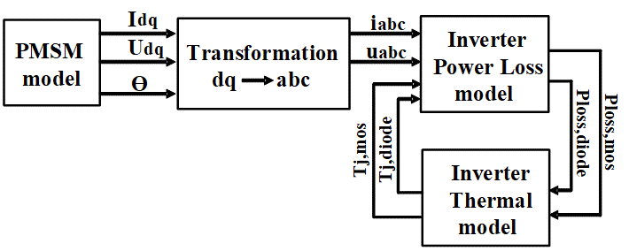 Figure 1: Overview of the system simulation model.
3. Conduction Losses including the MOSFET’s Reverse Conduction and Blanking Time
3.1. Conduction Losses in the SiC Power Module
The on-state losses for the investigated inverter are determined numerically using MATLAB. The methodology used in this work is based on the procedure presented in [6] and [32] for calculating the SiC MOSFETs’ conduction losses. In this procedure, the MOSFET on-state loss over a machine line period is determined according to
1 2?? 2 (??)??(??) ???? (1)
??????????,????????????????
here ?????? is the MOSFET on-state resistance, ???? the MOSFET current, ?? = 2?????? where ?? is the machine fundamental frequency and ?? is the duty cycle found as
??(??) = (1 + ?? sin ??) (2)
here ?? is the modulation index [33]. Similarly, the on-state losses of the diode can be formulated as
??????????,?? ????????(??))??(??) ???? (3)
From the data sheet, ????, the voltage drop and, ????, the on-state resistance can be found, ???? is the current through the diode.
The resulting expressions for the current through the MOSFET and the diode thus becomes
???? = ???????? sin????+(??−????????)−???? (4)
???? = ????????????sin??+(??−???????? )+???? (5)
where ?? is the angle of fundamental power factor and ???? is the peak value of the phase current [32].
The losses when incorporating and not incorporating the MOSFET reverse conduction are displayed in Figure 2 for the upper diode /MOSFET combination in a phase leg of a CAS300, SiC inverter. A substantial decrement of up to 83% in the diodes’ total on-state losses originating from the parallel conduction was found. In Table 1 the operating condition used for calculating the losses is given. Likewise, a reduction up to 97% is noticed in the total diodes’ conduction losses of the CAB450 SiC inverter.
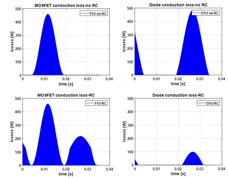 Figure 2: MOSFET and diode conduction losses with (RC), and without MOSFET reverse conduction (no RC), in CAS300 SiC inverter for upper MOSFET and diode in a phase leg.
Table 1: Chosen Operating Point of PMSM for Power Loss Calculations
| Variable | Value | Unit |
| Current magnitude | 565 | [A] |
| DC voltage | 300 | [V] |
| Blanking time | 0.5 | [µs] |
| Switching Frequency | 10 | [kHz] |
| Modulation index | 0.084 | [-] |
| Torque | 160 | [Nm] |
| Mechanical speed | 500 | [rpm] |
3.2. Blanking Time
The influence of blanking time is incorporated in the calculation of the on-state losses by formulating a representative duty cycle. The resulting formulation becomes,
??????(??) = ??(??) − ???????????????????????? = 12 (1 − 2???????????????????????? + ??????????) (6)
where ?????? is the switching frequency [32].
The calculated currents of the diodes and MOSFETs in a phase leg of the CAS300 inverter are presented in Figure 3, without (top one) and with (bottom one) utilizing blanking time, also incorporating the MOSFET reverse conduction. As can be seen in the bottom figure, there is current only in the diode for the blanking time intervals. This leads to an increase of 20 W (12%) in the diodes’ conduction losses for the CAS300 inverter which is alpha [rad]
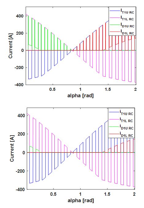 Figure 3 function of : Influence ?? =2??????of blanking time on in one phase leg of a CAS300 equipped inverter.
Both the diode and MOSFET currents as a when incorporating the MOSFET’s reverse conduction and not. Upper figure, no blanking time, lower figure with blanking time.
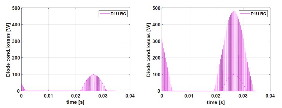 Figure 4: Diode conduction loss, without blanking time (left figure), with blanking time (right figure) in a phase leg of CAS300 SiC inverter.
4. Switching Losses
In SiC MOSFET illustrated in Figure 4 (right one). The impact on the MOSFETs’ conduction losses is very low. Likewise, for the CAB450, a rise of up to 70 W, of the diodes’ conduction losses is noted. Figure 4 presents the upper diode conduction loss in a phase leg of the CAS300, with and without blanking time, when incorporating the MOSFET reverse conduction. In Table 1 the operating condition used for the determination of the conduction losses are provided.
In the MOSFETs and its anti-parallel/body-diode, a resulting loss is created from each turn off and turn on. The switching losses in a MOSFET and diode can be obtained analytically by the expression as
??????.????????????,?????????? 1 ??
= ?????? ∙ ??????(@????????,????????) ∙ (?? ?????????? )????. (?????????????? )???? (7)
In the expression ?????? represents the switching energy loss, ???? the peak phase current, ???????? and ???????? the nominal current and voltage values and ???? , and ???? the current and voltage exponents [34]. In this study, in the numerical implementation, the switching loss is established at each switch-off and switch-on occasion of the module as
?????? ∑???? (8)
with ?? being the simulation time.
5. Electro-Thermal Calculation Network
Due to that several parameters in the modules are temperaturedependent, for instance the on-state resistances, forward voltage drops, switching and reverse recovery energies, the inverters’ power losses are determined through the usage of a thermal model, that is given in Figure 5. ????, are the junction temperatures of the MOSFET and the diodes, while ???? is the case temperature, ???? and ???? are the heatsink and fluid temperatures. In order to have a representative comparison, the same heatsink is utilized for both inverters. Noteworthy is that, for the inverters’ design, three SiC half-bridge modules were needed. All set-ups are normalized to a rated current of 600 A following the specification of the inverters.
Table 2: PMSM Rating Parameters
| Variable | Value | Unit |
| DC-Link voltage | 300 | [V] |
| Rated current | 400 RMS | [A] |
| Pole Pairs | 4 | [-] |
| Max. speed | 12000 | [rpm] |
| Max. torque | 160 | [Nm] |
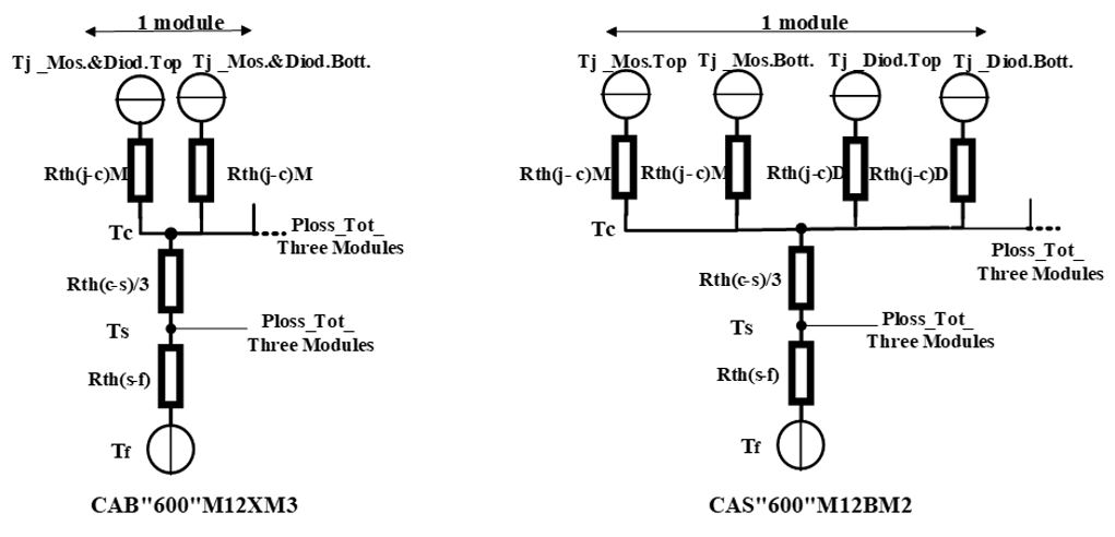 Figure 5: Thermal calculation model to find the power losses and temperatures.
The temperature and flow rate of the coolant is 65 ℃ and 10 L/min. Worth mentioning is that the latest 3rd GEN MOSFET dies have been used in the CAB450 module which have an intrinsic body diode, and accordingly the module does not need an antiparallel diode, as can be observed in Figure 5. In comparison, the CAS300 module is equipped with an anti-parallel Schottky diode.
6. Power Losses Analysis in SiC Inverters with and without Accounting for Thermal Feedback
As mentioned before, an operating point of a PMSM at high torque, low speed and high current magnitude is used to analyze the power losses of the two investigated SiC power modules. The chosen operating point can be noticed as the toughest operating condition in the urban driving cycles. MPTA/MTPV field-oriented control is utilized to generate the inverter currents. Based on this control strategy, the machine operates in the constant torque speed range and in the partial and full field weakening speed ranges [35,36]. Table 1 gives the chosen operating point and key machine parameters are given in Table 2. As depicted in Figure 1, an iterative approach is used to find the losses based on the temperature in which, the devices’ steady-state and transient parameters (????, ????, ????, ????, ??????, ?????? and ??????) are interpolated using the feedback of the junction temperature. The losses and the temperatures are looped until they have converged. Worth mentioning is that the switching energies of the devices are interpolated as a function of junction temperature and current to fulfill both the current and temperature dependency of the switching energies. The results of the investigations are given in Table 3. It is worth to note that, for a fair comparison, a power loss scaling factor is utilized on the SiC modules in order to form them into 600 A modules.
As shown in Table 3, a significant reduction in diode conduction losses is observed for the two SiC modules. As was explained in sections 2 and 3, this is due to the MOSFET’s reverse conduction ability to utilize the diode and the MOSFET to share the current. In the SiC modules, the increase of on-state losses for the built-in diodes as a function of an increase in junction temperature is substantially lower compared to that of the MOSFETs’ channel. This is due to a more moderate rise in the diode dynamic resistance with respect to the temperature increase. Moreover, for the two investigated modules, in SiC-MOSFETs, a temperature increase has almost zero effect on the switching losses.
For the comparison of the two SiC modules, a substantial decrease is noticed in the on-state losses in the CAB450’s diodes. This is due to the fact that, the CAB450 module is using the latest 3rd GEN MOSFET dies with a very robust intrinsic body diode and reliable operation in the 3rd quadrant. This feature is weaker in the CAS 300 Module.
All in all, the analysis shows that the thermal feedback has a considerable impact on the losses and leads to an increase of up to 11% for CAS300 and 15.6% for CAB450 on the inverters’ total conduction losses at the chosen operating condition. This leads to that the demand for effective cooling strategies of the semiconductor power modules is increasing continuously, especially for traction applications which can typically have a high ambient temperature, particularly in SiC-MOSFETs where the temperature variations have larger magnitudes compared to those of Si-IGBTs [37]. Hence, in the following sections, utilizing graphene, a novel thermal conductive, cost-effective, and ecofriendly material is proposed in the power module packaging and
Table 3: Calculated Average Values of Conduction and Switching Losses of the SiC Inverters utilizing and not utilizing Thermal Feedback, Considering Blanking Time and using the MOSFET’s Reverse Conduction at 160 Nm, 500 rpm Mechanical Speed and ???? =65℃.
CAB “600”M12XM3 (CAB450)
Cond. Cond. Diff. Diff.% Sw. Sw. Diff. Diff.% Tjunc.
[W] Thermal [W] [W] Thermal [W] Thermal
Feedback Feedback Feedback
[W] [W] [℃] MOSFETs 977.8 1140.5 162.7 16.6 206.6 206.8 0.2 0.09 99.8
Diodes 74.4 75.4 1 1.35 3.51 3.52 0.01 0.28 99.8
Tot. Inverter 1052.2 1215.9 163.7 15.6 210.1 210.3 0.22 0.1
CAS “600”M12BM2 (CAS300)
Cond. Cond. Diff. Diff.% Sw. Sw. Diff. Diff.% Tjunc.
[W] Thermal [W] [W] Thermal [W] Thermal
Feedback Feedback Feedback
[W] [W] [℃] MOSFETs 1072 1164 92 8.6 196.3 196.5 0.2 0.1 95.6
Diodes 140.1 182.1 42 29.9 0 0 0 0 88.2
Tot. Inverter 1212.1 1346.1 134 11 196.3 196.5 0.2 0.1
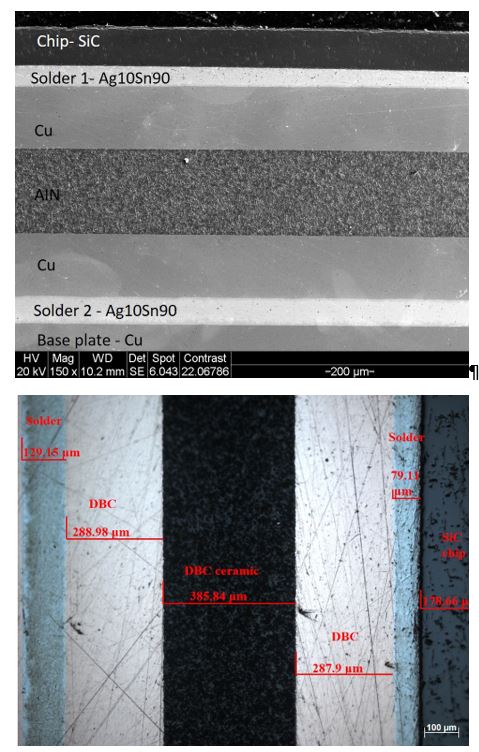 Figure 6: The Layer materials of the reference SiC module CAS300 from SEM and ESD analyses (top) and the materials respective thickness of CAS300 from SEM and ESD analyses (bottom) (given in Table 4).
analyzed by FEM in the COMSOL Multiphysics software intended to improve the heat spreading inside the module.
7. 3D-CAD Model and Thermal Modeling Set-up of the Power Module using SEM and EDS Analyses
As was mentioned before, to enhance the heat spreading and cooling of the semiconductor chips in the chosen half-bridge SiC power module, CAB450M12XM3, a thermal model is built up as close as possible to the real module starting from CAD and then FEM simulation in COMSOL Multiphysics. Even though the thermal packaging aspects of the module was mostly unknown due to confidentiality. However, the key features were known from the reverse engineering effort, which showed that the base plate and insulator have been made of copper and silicon nitride, respectively. Therefore, a Scanning Electron Microscopy (SEM) together with an Energy Dispersive X-Ray Spectroscopy (EDS) investigation were conducted on the available similar voltage class SiC power module, CAS300M12BM2, as a reference to approximate further material information. EDS is a chemical micro-analysis technique, which identifies the x-rays released from the sample through a bombardment process with electrons, so that the element arrangement of the analyzed volume can be found. The above-mentioned analyses have been conducted on a cross-sectional cut off piece of the module. As illustrated in Figure 6 (top), the chips are all silicon-carbide, the base plate is made of copper and an aluminum nitride (AIN) insulator has been used as one of the DBC layers. The other two DBC layers are made of copper. Moreover, the solder Sn90Ag10 is used for both solder layers. The thickness of the layers which is shown in Figure 6 (bottom), is given in Table 4.
In the next step, the CAD geometry of the CAB450 SiC power module including the thermal aspects is meshed in COMSOL Multiphysics based on the SEM and EDS analyses data from the reference CAS300 module as well as the CAB450 datasheet information. Instead of AIN, silicon nitride (Si3N4) is used as the ceramic material in the DBC substrate based on the CAB450 datasheet. Figure 7 (left) presents a 3D-geometry of the CAB450 half-bridge power module including the chips in which each group of five chips is representing one SiC switch place. The dimensions are implemented according to the datasheet information.
8. Automized FEM Computation in COMSOL for Steady- state/Transient Heat Dissipation
As mentioned before, to be able to capture all the heat dissipation surface interactions, a 3D FEM simulation in COMSOL Multiphysics is performed. Each of the power module materials and their thicknesses were accounted for in the meshing procedure as separate computational domains including the solders, copper, DBC, etc. In order to take the thermal coupling and heat spreading effects into consideration, the contact resistances among the material layers were also modelled using the provided realistic values by material datasets. As the focus of the analysis is on the thermal distribution through the chips and DBC layers, a manually refined mesh is applied in these domains. Overall, a uniform mesh distribution is built up as depicted in Figure 7 (right). The boundary conditions are caried out by considering the chips as heat sources and a selected power losses of 1262 W, i.e., 126.2 W per chip from the previous power loss calculations of the investigated module is applied to these heat sources.
Table 4: Power Module Layers’ Thicknesses and Thermal Properties
| Layer | Material | Thickness (μm) | Thermal conductivity,
K (W/m.K) |
Density, ρ (kg/m3) | Heat capacity, C (J/kg.K) |
| Chip | SiC | 178 | 490 | 3216 | 690 |
| DBC | Cu | 288 | 400 | 8940 | 385 |
| DBC ceramic | AIN/Si3N4 | 386 | 20 | 3100 | 700 |
| Solder (below the chip)/ (below the DBC layer) | Sn90Ag10 | 79/129 | 50 | 9000 | 150 |
| Baseplate | Cu | 3 | 400 | 8940 | 385 |
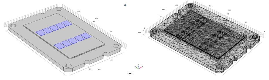 Figure 7: 3D-geometry of CAB450 SiC module built for simulation (left) and the mesh visualization of the module (right).
To mimic a liquid cooling solution, the bottom surface of the baseplate is given a heat transfer coefficient of 3000 W/(m2.K) to represent the convective heat flux as a boundary condition with a liquid flow of water with a rate of 1 m/s (one meter per second) and a temperature of 65°C. All other boundaries are set to have a heat transfer coefficient of 10 W/(m2.K), which is the convection of low-speed air flow above a surface [38].
In general, the transportation of heat can be described as the transportation of the thermal energy as a result of a gradient in temperature. Then the heat flux can be expressed by Fourier’s law as
?? = −?? ∇?? (9)
which defines the theory behind the heat conduction. The equation shows that the thermal conductivity, ?? in (W/m.K), is proportional to the magnitude of the temperature gradient. ?? is the heat flux measured in (W/m2) and ∇?? is the temperature gradient.
The heat convection, which can either be natural or forced, is added to the boundaries of the system, and is dependent on the geometry and its length. When natural convection is implemented, the system is cooled naturally through air. The steady-state heat flux density is calculated as the following equation
???? = ℎ (???? − ????) (10)
when the convective cooling/heating is involved. ℎ is the heat transfer coefficient in W/(m2.K), ???? represents the surface temperature and ???? is the media temperature.
Since there are different materials involved in this study, then the heat conduction or heat diffusion must be taken into account by the expression as
???? ???????? = ∇??(??)∇T + ???? (11)
where ?? is the density, C is the heat capacity, ???? represents the
???? difference of temperature over time, and ∇T is the temperature gradient.
Finally, the model is ready for analyzing the time variations of the temperature inside the different layers of the power module and the temperature profiles across it, within the boundary layers. The first results will illustrate the thermal performance of the investigated power module which is built up as close as possible to the real model and in the next phase an assembled graphene film layer is placed under the first copper layer as close as possible to the chips as heat sources to demonstrate the improvement of the heat distribution inside the module from the chip level towards the different layers.
9. Results of Steady-state Thermal Computation of the Power Module
The stationary solver in COMSOL is used to evaluate the steady-state temperature distribution across the power module from the chips towards the bottom layers. The heat distribution is measured by applying a 3D-cutline from the middle chip to the baseplate as depicted in Figure 8. The reason for choosing the middle chip is since this one will experience the highest thermal stress. As it can be seen in Figure 9 (top), the result shows an average maximum temperature of around 99°C for the chips for the applied power loss of 126.2 W per chip which is approximately close to the junction temperature calculated by the electro-thermal model presented in section 6, Table 3. The lowest temperature of 70°C is also noticed around the edges of the module. The temperature profile across all the layers is illustrated in Figure 9 (bottom).
In addition, the thermal resistance of the junction to case ( ????ℎ????) of 0.2 K/W has been obtained from the simulation.
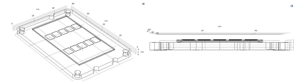 Figure 8: 3D-cutline across the module for temperature measurements, top view (left) and side view (right).
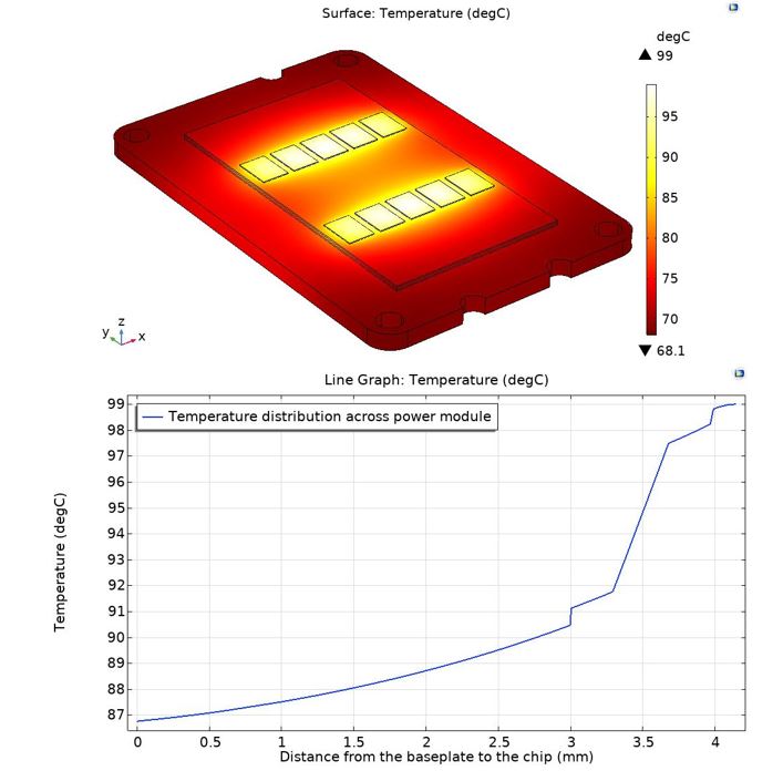 Figure 9: Temperature distribution across the power module (top) and temperature profile across all the layers (bottom).
As mentioned before, a novel solution to efficiently transport the heat away from the power devices, especially in high power applications can be achieved by integrating ultra-high thermal conducting as well as flexible and robust materials into the cooling path [7]. Therefore, graphene which is one of the most promising materials that can provide the above-mentioned properties, has been used in this study to optimize the thermal impedance of the power module as well as to make a uniform and fast heat spreading over the module.10. Using the Graphene Assembled Film in the module Packaging
To prove this goal, the graphene layer has been placed as close as possible to the chips which are the heat sources, with an in-plane thermal conductivity of 2900 W/m.K in x and y directions and a cross-plane thermal conductivity of 14 W/m.K in the z direction. The directions as the design parameters should be chosen in such a way that they conduct and spread the heat flow as fast and
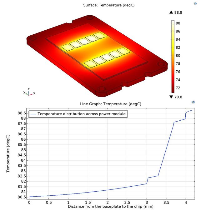 Figure 10: Temperature distribution across the power module (top) and temperature profile across all the layers (bottom) with graphene.
Table 5: Graphene Thermal Properties
| Material | Thermal conductivity,
K (W/m.K) |
Density ρ (kg/m3) | Heat capacity, C
(J/kg.K) |
| Graphene | (x,y,z) = (2900,2900,14) | 2267 | 720 |
efficient as possible on the surface of the module and then towards the bottom layers.
Worth mentioning is that, to reach high performing thermal and mechanical properties, the fabricating freestanding graphene films (GFs) have shown a promising potential compared to using single/few layer graphene for the thermal management of high-power electronics [7]. Hence, in this work, 1 μm thick graphene films are utilized to make an appropriate layer thickness in respect to the thermal conductivity which is challenging since the thermal conductivity levels are very much dependent on the thickness of the graphene layer [7]. The layer is placed under the first copper layer as a realistic placement in order to not weaken the electrical conductivity through the module which otherwise might happen as a result of a poor insulating ability of the graphene material.
In addition, in the fabrication processes, in order to minimize the thermal contact resistance between the graphene layer and other different substrates, a molecular functionalization method is used in which the small molecules are utilized to functionalize the surface of the graphene film which is in contact with the device surfaces. The small molecule, as the functional agent, gives as result a formation of molecular bridges between the device substrates and the grapheme-based surface and in this way the thermal resistance between these layers is strongly reduced [39].
Therefore, based on this method, the contact resistance is set to 1.1 × 10⁻⁸ K.m2/W in this work to achieve the appropriate thermal coupling between the layers [39]. Table 5 gives the material properties of graphene.
Results of Steady-state Thermal Computation of the Power Module with Graphene Layer
To investigate the thermal behavior in the presence of the graphene layer in the power module, a 3D-cutline from the middle chip to the baseplate, similar as in section 9 is applied to the module.
The result reveals a reduction of 10°C in the average temperature per chip for the applied power loss of 126.2 W per chip, as depicted in Figure 10, and Figure 10 (bottom) which illustrates the temperature profile across all the layers. Moreover, as can be seen in Figure 11, a comparison between the two cases,
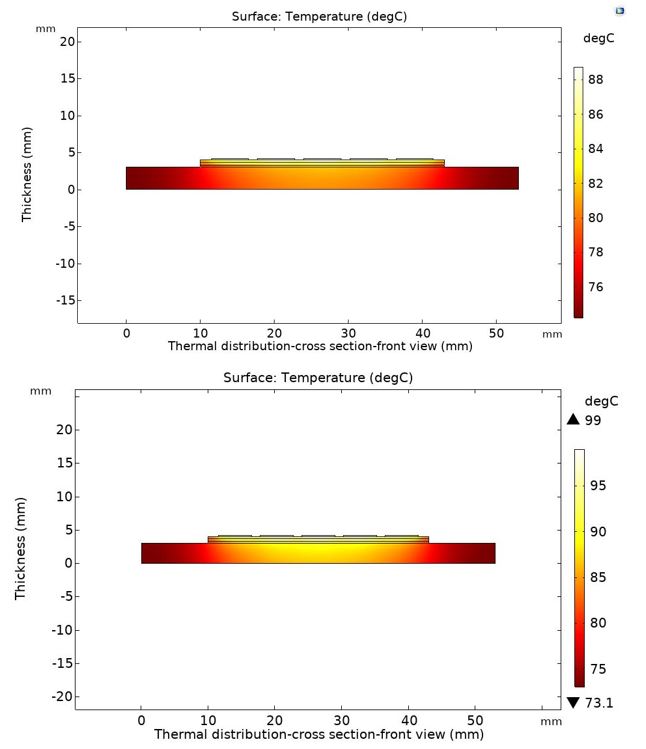 Figure 11: Temperature distribution with graphene (top) and without graphene (bottom). with and without using graphene, confirms the expected results,
Moreover, Figure 12 depicts the temperature distribution across each layer which clearly shows the temperature difference of more than 10°C between the two cases for the applied power loss per chips.i.e., a noticeable difference in the temperature distribution in the module. With graphene (top figure), the temperature is spreading flatter and more homogeneously in each layer, which means that each layer is absorbing the heat uniformly. Consequently, the heat is more distributed across the baseplate compared to that of the case without graphene (bottom figure) in which the heat is mostly concentrated in the middle where the chips are located. Therefore, this temperature uniformity leads to a significant improvement, 54.3%. The junction to case thermal resistance ( ????ℎ????) equals to 0.0913 K/W, using the graphene layer compared to that of 0.2 K/W without graphene.
12. Transient Thermal Computation of the Power Module,
Since the load of the inverter is constantly varying, hence real-time thermal computations are necessary to more accurately quantify the thermal behavior and reliability of the inverters. with/without Graphene layer using WLTC Driving Cycle Therefore, the time-dependent solver in COMSOL is used to evaluate the transient temperature distribution across the power module from the chips towards the bottom layers over the WLTC driving schedule consisting of both the urban and highway phases. Currently in many countries including the EU, WLTC is the main drive test procedure for light-duty vehicles. First based on the vehicle model used in this study, the required torque and speed values for the PMSM model are determined. The values are then utilized for the power loss calculation over the WLTC drive test
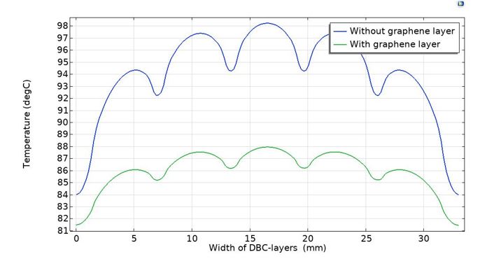 Figure 12: Temperature distribution across each layer with/without graphene.
| Vehicle Parameter | Value | Unit |
| Total mass of the vehicle | 1700 | [kg] |
| Aerodynamic drag coefficient | 0.35 | [-] |
| Vehicle cross section area | 2 | [m^2] |
| Rolling friction coefficient | 0.007 | [-] |
| Wheel radius | 0.3 | [m] |
Table 6: Vehicle Parameters Figure 13 illustrates the calculated power losses in the WLTC, and Figure 14 shows the temperature distribution across the power module for the two cases (with/without) graphene. The thermal profile comparison per chip between the case of the power module with the assembled graphene film and without the graphene film is depicted in Figure 15. As can be seen in Figure 13, the highest calculated power losses are observed around 1000 second for the
related speeds and torques of the PMSM based on the used vehicle and thereafter for the thermal loading in COMSOL. Table 6 gives model parameters. Therefore, the temperature distributions for the the vehicle model parameters. two cases, with/without graphene are considered at 1033 s.
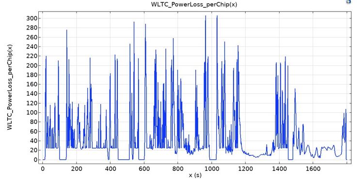
Figure 13: Calculated power losses over WLTC
In order to measure the transient heat distribution, a 3D-cutline from the middle chip to the baseplate is used similarly as done in the steady-state simulation and then the calculated power losses over WLTC are applied to the chips as the heat sources.
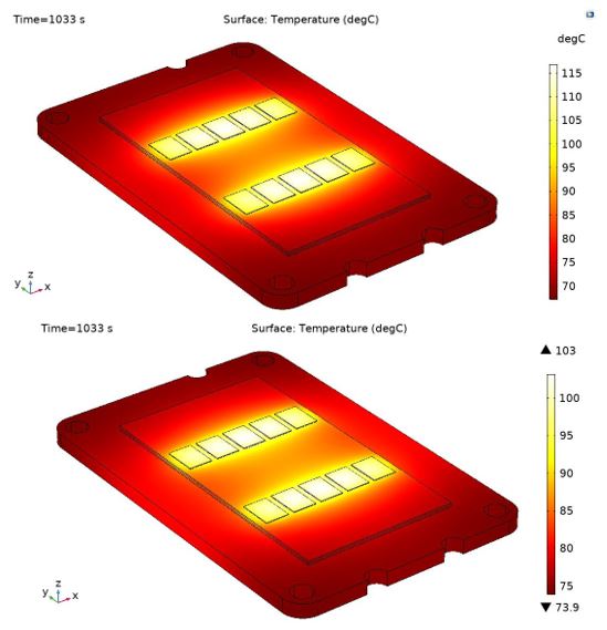 Figure 14: Temperature distribution across the power module without the graphene layer (top) and with the graphene layer (bottom) at 1033 s.
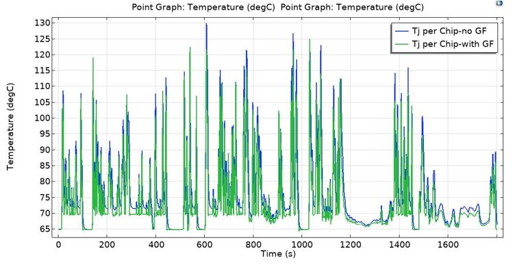 Figure 15: Comparison of the average junction temperature profile of each chip over the WLTC drive cycle.
According to Figure 14, a temperature reduction of about 15°C per chip at 1033 s is observed in case of using the graphene layer in the power module. Moreover, a close look into the heat distribution over the module shows a flatter distribution in case of using graphene. Also, with graphene the heat is more distributed across the baseplate compared to the case without graphene in which the heat is more concentrated in the middle, where the chips are located. Quite clearly proven, graphene as a heat conductor is improving the heat spreading across the module and this leads to an effectivization of the cooling of the semiconductor power module.
Finally, Figure 15 illustrates the thermal profile comparison over the WLTC driving schedule per chip between the two cases, with and without the graphene layer. As depicted, the graphene layer gives a lower average junction temperature per chip and this can lead to a lower operating temperature of the semiconductor power module in general. Worth mentioning is that this effect can be more apparent in high-power applications where due to the high voltage and current levels used, a high number of chips are needed. Also, as observed before in the steady-state simulation, boosting the heat dissipation performance in the chips and power module by using graphene, leads to a noticeable reduction in the junction to case thermal resistance of the power module and decreasing the operating temperature accordingly.
13. Conclusion
In this paper, the impact of neglecting the thermal feedback on the conduction losses for two SiC inverters were determined. The effect is demonstrated for a chosen heavy operating point of a PMSM, high torque and low speed, which is a difficult operating point from a power loss perspective. Since accounting for the thermal feedback shows a considerable increase in the inverter total conduction losses, therefore, graphene as a novel thermal management material is utilized as a layer in the power module packaging to improve the thermal dissipation and cooling of the SiC chips in the power module. A steady- state as well as a transient thermal computation in COMSOL Multiphysics are carried out on the investigated SiC power module which is created in a way to be as close as possible to a real module in terms of layers material, electrical and thermal aspects.
The thermal computation results imply a noticeable improvement in thermal spreading over the module which leads to a lower thermal resistance from junction to case of the module and a lower operating temperature in both the steady-state and transient computations. The transient computations have been applied over a WLTC drive cycle to investigate the thermal variations of the SiC chips when the load varies in a hybrid vehicle powertrain.
Worth mentioning is that, inserting the graphene assembled films in the SiC power module and functionalizing the films to reduce the contact thermal resistances in a standard electronics lab is very challenging due to a very thin and flexible texture of the graphene material. In addition, different variables including the inner temperatures, the heat distribution, and the streamlines, etc., within the multiple layers from the SiC chips down to the whole bottom layers cannot be easily measured on the hardware implementation even with many sensors. Therefore, using FEM in COMSOL Multiphysics is found to be a reliable method to simulate the thermal aspects precisely and prove the concepts of this paper.
To sum up, with this study, the application of using graphene in the building of the power module demonstrates a promising potential to boost the heat spreading in the semiconductor power modules especially in the high-power applications where also lightweight is required as priority in the light-duty vehicles.
As most important future work, measurement verification is the next step.
Conflict of Interest
The authors declare that they have no known competing financial interests or personal relationships that could have appeared to influence the work reported in this article.
- J. Reimers, L. Dorn-Gomba, C. Mak, A. Emadi, “Automotive traction inverters: Current status and future trends,” IEEE Transactions on Vehicular Technology, 68(4), 3337–3350, 2019.
- K. Kumar, M. Bertoluzzo, G. Buja, “Impact of SiC MOSFET traction inverters on compact-class electric car range,” in 2014 IEEE International Conference on Power Electronics, Drives and Energy Systems (PEDES), 1–6, 2014, doi:10.1109/PEDES.2014.7042156.
- J. Biela, M. Schweizer, S. Waffler, J.W. Kolar, “SiC versus Si—Evaluation of Potentials for Performance Improvement of Inverter and DC–DC Converter Systems by SiC Power Semiconductors,” IEEE Transactions on Industrial Electronics, 58(7), 2872–2882, 2011, doi:10.1109/TIE.2010.2072896.
- K. Olejniczak, T. McNutt, D. Simco, A. Wijenayake, T. Flint, B. Passmore, R. Shaw, D. Martin, A. Curbow, J. Casady, B. Hull, “A 200 kVA electric vehicle traction drive inverter having enhanced performance over its entire operating region,” in 2017 IEEE 5th Workshop on Wide Bandgap Power Devices and Applications (WiPDA), 335–341, 2017, doi:10.1109/WiPDA.2017.8170569.
- S.E. Schulz, “Exploring the High-Power Inverter: Reviewing critical design elements for electric vehicle applications,” IEEE Electrification Magazine, 5(1), 28–35, 2017, doi:10.1109/MELE.2016.2644281.
- J. R?bkowski, T. P?atek, “Comparison of the power losses in 1700V Si IGBT and SiC MOSFET modules including reverse conduction,” in 2015 17th European Conference on Power Electronics and Applications (EPE’15 ECCE-Europe), 1–10, 2015, doi:10.1109/EPE.2015.7309444.
- J.L. Nan Wang, Majid Kabiri Samani, Hu Li, Lan Dong, Zhongwei Zhang, Peng Su, Shujing Chen, Jie Chen, Shirong Huang, Guangjie Yuan, Xiangfan Xu, Baowen Li, Klaus Leifer, Lilei Ye, Tailoring the Thermal and Mechanical Properties of Graphene Film by Structural Engineering, Small, 14(29), 1801346, doi:10.1002/smll.201801346.
- T.M. Tritt, Thermal conductivity?: theory, properties, and applications, Springer, 2010.
- L. Peng, Z. Xu, Z. Liu, Y. Guo, P. Li, C. Gao, “Ultrahigh Thermal Conductive yet Superflexible Graphene Films,” Advanced Materials, 29(27), 2017, doi:10.1002/ADMA.201700589.
- A.A. Balandin, S. Ghosh, W. Bao, I. Calizo, D. Teweldebrhan, F. Miao, C.N. Lau, “Superior thermal conductivity of single-layer graphene,” Nano Letters, 8(3), 902–907, 2008, doi:10.1021/NL0731872.
- Y. Liu, S. Chen, Y. Fu, N. Wang, D. Mencarelli, L. Pierantoni, H. Lu, J. Liu, “A lightweight and high thermal performance graphene heat pipe,” Nano Select, 2, 2020, doi:10.1002/nano.202000195.
- N.J. Song, C.M. Chen, C. Lu, Z. Liu, Q.Q. Kong, R. Cai, “Thermally reduced graphene oxide films as flexible lateral heat spreaders,” Journal of Materials Chemistry A, 2(39), 16563–16568, 2014, doi:10.1039/C4TA02693D.
- G. Xin, H. Sun, T. Hu, H.R. Fard, X. Sun, N. Koratkar, T. Borca-Tasciuc, J. Lian, “Large-area freestanding graphene paper for superior thermal management,” Advanced Materials, 26(26), 4521–4526, 2014, doi:10.1002/ADMA.201400951.
- Z. Liu, Z. Li, Z. Xu, Z. Xia, X. Hu, L. Kou, L. Peng, Y. Wei, C. Gao, “Wet-spun continuous graphene films,” Chemistry of Materials, 26(23), 6786–6795, 2014, doi:10.1021/CM5033089.
- J. Li, F. Ye, S. Vaziri, M. Muhammed, M.C. Lemme, M. Östling, “Efficient inkjet printing of graphene,” Advanced Materials, 25(29), 3985–3992, 2013, doi:10.1002/ADMA.201300361.
- Y. Fu, J. Hansson, Y. Liu, S. Chen, A. Zehri, M.K. Samani, N. Wang, Y. Ni, Y. Zhang, Z. Bin Zhang, Q. Wang, M. Li, H. Lu, M. Sledzinska, C.M.S. Torres, S. Volz, A.A. Balandin, X. Xu, J. Liu, “Graphene related materials for thermal management,” 2D Materials, 7(1), 2020, doi:10.1088/2053-1583/AB48D9.
- N. Wang, Y. Liu, S. Chen, L. Ye, J. Liu, “Highly Thermal Conductive and Electrically Insulated Graphene Based Thermal Interface Material with Long-Term Reliability,” in 2019 IEEE 69th Electronic Components and Technology Conference (ECTC), 1564–1568, 2019, doi:10.1109/ECTC.2019.00240.
- M.F. Abdullah, S.A. Mohamad Badaruddin, M.R. Mat Hussin, M.I. Syono, “EVALUATION ON THE REDUCED GRAPHENE OXIDE THERMAL INTERFACE MATERIAL AND HEAT SPREADER FOR THERMAL MANAGEMENT IN HIGH-TEMPERATURE POWER DEVICE,” Jurnal Teknologi, 83(3 SE-), 53–59, 2021, doi:10.11113/jurnalteknologi.v83.15102.
- J.S. Lewis, Reduction of Device Operating Temperatures with Graphene-Filled Thermal Interface Materials, C , 7(3), 2021, doi:10.3390/c7030053.
- Y. Liu, T. Thiringer, N. Wang, Y. Fu, H. Lu, J. Liu, “Graphene based thermal management system for battery cooling in electric vehicles,” in 2020 IEEE 8th Electronics System-Integration Technology Conference (ESTC), 1–4, 2020, doi:10.1109/ESTC48849.2020.9229856.
- N. Wang, Y. Liu, L. Ye, J. Li, “Highly Thermal Conductive and Light-weight Graphene-based Heatsink,” in 2019 22nd European Microelectronics and Packaging Conference Exhibition (EMPC), 1–4, 2019, doi:10.23919/EMPC44848.2019.8951839.
- S. Huang, Y. Zhang, S. Sun, X. Fan, L. Wang, Y. Fu, Y. Zhang, J. Liu, “Graphene based heat spreader for high power chip cooling using flip-chip technology,” in 2013 IEEE 15th Electronics Packaging Technology Conference (EPTC 2013), 347–352, 2013, doi:10.1109/EPTC.2013.6745740.
- S. Huang, Y. Zhang, N. Wang, N. Wang, Y. Fu, L. Ye, J. Liu, “Reliability of graphene-based films used for high power electronics packaging,” in 2015 16th International Conference on Electronic Packaging Technology (ICEPT), 852–855, 2015, doi:10.1109/ICEPT.2015.7236714.
- S. Huang, J. Bao, H. Ye, N. Wang, G. Yuan, W. Ke, D. Zhang, W. Yue, Y. Fu, L. Ye, K. Jeppson, J. Liu, “The effects of graphene-based films as heat spreaders for thermal management in electronic packaging,” in 2016 17th International Conference on Electronic Packaging Technology (ICEPT), 889–892, 2016, doi:10.1109/ICEPT.2016.7583272.
- P. Zhang, N. Wang, C. Zandén, L. Ye, Y. Fu, J. Liu, “Thermal characterization of power devices using graphene-based film,” in 2014 IEEE 64th Electronic Components and Technology Conference (ECTC), 459–463, 2014, doi:10.1109/ECTC.2014.6897324.
- M.R.M. Hussin, M.M. Ramli, S.K.W. Sabli, I.M. Nasir, M.I. Syono, H.Y. Wong, M. Zama, “Fabrication and characterization of graphene-on-silicon schottky diode for advanced power electronic design,” Sains Malaysiana, 46(7), 1147–1154, 2017, doi:10.17576/JSM-2017-4607-18.
- J. Wang, L. Shi, Y. Li, L. Jin, Y. Xu, H. Zhang, Y. Zou, Y. Lan, X. Ma, “Thermal management of graphene-induced high-power semiconductor laser package with bidirectional conduction structure,” Optics and Laser Technology, 139, 2021, doi:10.1016/J.OPTLASTEC.2021.106927.
- K. Hemanjaneyulu, M. Khaneja, A. Meersha, H.B. Variar, M. Shrivastava, “Comprehensive Computational Modelling Approach for Graphene FETs,” in 2018 4th IEEE International Conference on Emerging Electronics (ICEE), 1–5, 2018, doi:10.1109/ICEE44586.2018.8937909.
- S. Amirpour, T. Thiringer, D. Hagstedt, “Power Loss Analysis in a SiC/IGBT Propulsion Inverter Including Blanking Time, MOSFET’s Reverse Conduction and the Effect of Thermal Feedback Using a PMSM Model,” in IECON 2020 The 46th Annual Conference of the IEEE Industrial Electronics Society, 1424–1430, 2020, doi:10.1109/IECON43393.2020.9254297.
- Wolfspeed, CAB450M12XM3, Nov. 2021.
- Wolfspeed, CAS300M12BM2, Nov. 2021.
- A. Acquaviva, T. Thiringer, “Energy efficiency of a SiC MOSFET propulsion inverter accounting for the MOSFET’s reverse conduction and the blanking time,” in 2017 19th European Conference on Power Electronics and Applications (EPE’17 ECCE Europe), P.1-P.9, 2017, doi:10.23919/EPE17ECCEEurope.2017.8099052.
- J.W. Kolar, H. Ertl, F.C. Zach, “Influence of the modulation method on the conduction and switching losses of a PWM converter system,” IEEE Transactions on Industry Applications, 27(6), 1063–1075, 1991, doi:10.1109/28.108456.
- SEMIKRON, Application Manual Power Semiconductors, Ilmenau, 2015.
- M. Meyer, J. Bocker, “Optimum Control for Interior Permanent Magnet Synchronous Motors (IPMSM) in Constant Torque and Flux Weakening Range,” in 2006 12th International Power Electronics and Motion Control Conference, 282–286, 2006, doi:10.1109/EPEPEMC.2006.4778413.
- M. Meyer, T. Grote, J. Bocker, “Direct torque control for interior permanent magnet synchronous motors with respect to optimal efficiency,” in 2007 European Conference on Power Electronics and Applications, 1–9, 2007, doi:10.1109/EPE.2007.4417370.
- L. Ceccarelli, R.M. Kotecha, A.S. Bahman, F. Iannuzzo, H.A. Mantooth, “Mission-Profile-Based Lifetime Prediction for a SiC mosfet Power Module Using a Multi-Step Condition-Mapping Simulation Strategy,” IEEE Transactions on Power Electronics, 34(10), 9698–9708, 2019, doi:10.1109/TPEL.2019.2893636.
- E. EDGE, Convective heat transfer coefficients table chart, Nov. 2021.
- H. Han, Y. Zhang, N. Wang, M.K. Samani, Y. Ni, Z.Y. Mijbil, M. Edwards, S. Xiong, K. Sääskilahti, M. Murugesan, Y. Fu, L. Ye, H. Sadeghi, S. Bailey, Y.A. Kosevich, C.J. Lambert, J. Liu, S. Volz, “Functionalization mediates heat transport in graphene nanoflakes,” Nature Communications, 7(1), 11281, 2016, doi:10.1038/ncomms11281.
No related articles were found.