Stability Analysis of a DC Microgrid with Constant Power Load

Adv. Sci. Technol. Eng. Syst. J. 7(2), 63–72 (2022);
 DOI: 10.25046/aj070206
DC Microgrids (DCMGs) aggregate and integrate various distribution generation (DG) units through the use of power electronic converters (PECs) that are present on both the source side and the load side of the DCMGs. Tightly regulated PECs at the load side behave as constant power loads (CPLs) and may promote instability in the entire DCMG. Previous research has mostly focused on devising stabilization techniques with ideals CPLs that may not be feasible to realize; few publications that emulate DCMG stability with practical CPLs are restricted in application because they add components that considerably increase the cost of the DCMGs. This study aims at stabilizing the DCMG in the presence of practical CPL in a way that is economically feasible, i.e., without the addition of complex compensators. This paper presents a Simulink model of the smallest DCMG, i.e., a cascaded DC-DC power converter network with a practical CPL assumed at the load side of the network. Using theoretical calculations and computer simulations, we have determined the suitable CPL power level and the bandwidth of the current controller at which the smallest DCMG is stable. We have performed the stability analysis of the source side buck converter and the CPL with the derived power level and bandwidth, and found that individual converter systems are stable, thereby proving that the entire DCMG is stable despite the presence of a CPL.
1. Introduction
In recent times, the demand for DCMGs is surging. With this, there are significant issues related to the distribution networks in the power systems. The preliminary analysis and results of one such issue i.e., caused due to CPL is done in [1]. There are other associated problems like voltage fluctuations, there is a need to aggregate DG units and provide proper coordination. Thus, the development of microgrids becomes indispensable to integrate and coordinate different power systems. US department of energy, DoE defines microgrids as “Locally confined and independently controlled electric power grids in which distribution architecture integrates loads and distributed energy resources which allows the microgrid to operate connected or isolated to a main grid” [2].
While microgrids can be developed for both AC and DC supplies, DCMGs are considered superior to the AC microgrids due to several factors. The DC networks sidestep reactive power issues, which simplifies the control loop design [3]. It also results in reduced hardware (power cables), thereby reducing the overall equipment cost. Further, DCMG implementation eliminates long transmission and distribution lines that aids in providing reliable and efficient DG system [4]. Also, in recent times, integration of renewable energy sources, fuel cells, and energy storage devices with conventional power systems has become indispensable. The urgency of these issues has brought DC power systems back into picture through DCMGs. DCMGs consist of power electronic elements that are used for various purposes. For example, they can be used to isolate the microgrid from the main power system, or to make a network of distributed generation systems that need to be synchronized. These are termed as multi-converter power electronic systems [5, 6] that employ power converters to control various grid parameters like voltage, current, power, etc.
A DC distribution system has two broad stages as shown in Figure 1 [7]. The first stage consists of two or more converters that are connected in parallel and feeding the DC bus [7]. These are switched mode power supplies (SMPS1) called line regulating converters (LRC) or source side converters. This converter system feeds the DC bus with a regulated voltage; the bus is further connected to another set of switched mode power supplies (SMPS2) called point of load (POL) converters, or load side converters. It has been shown that tightly regulated POLs behave as constant power loads (CPLs). Theoretically, the power supplied to the CPL equals the product of output voltage of the CPL and the current flowing through it. When the power supplied in a CPL is constant, then the voltage varies inversely with respect to the current change. Thus, the voltage increases when the current decreases and vice versa thereby resulting in negative incremental impedance. This concludes that the constant power loads exhibit a non-linear phenomenon that causes instability in DCMGs. Moreover, solving the stability issue becomes challenging when at least two power converters are cascaded to each other. Previous literature has considered load side power converters to be behaving as ideal CPLs. As a result, study of power levels and dynamic performance of CPL and how they affect system stability has been mostly neglected. Hence, it becomes important to investigate the system stability and evaluate the technical restrictions of CPL.
This paper seeks to study what technical restrictions can be levied on CPL to ensure stability of the DCMG. To do the analysis, a simulation scheme of source side buck converter and CPL is designed. The choice of this buck topology has been reinforced by two main reasons: i) Buck topology has simple construction and dynamic performance, and ii) It has higher system stability than boost or buck-boost topology. The rest of this paper is organized as follows: sections II and III discusses the design and design of source side buck converter. Sections IV and V discusses the stability analysis and design of the CPL. Section VI discusses the cascading of the source side buck converter and CPL to form the smallest DCMG. Appendix and section VII show the simulation models developed and their corresponding results respectively. The conclusion is mentioned in section VIII.
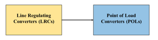 Figure 1: Major Components of DC distribution system
2. Controller Design for Source Side Buck Converter
In the research literature, linear droop control is realized through a virtual or an actual resistor in series with the DC-DC converters that are modeled as voltage sources. While droop control is a practical and viable voltage control scheme to regulate a constant DC voltage supply, it may work for buck converter topology [7]. Whereas the equivalent circuit of a converter in other topologies consists of transformers with nonlinear turn ratios, this will hinder the use of linear droop control for such converters [8]. Thus, to implement linear droop scheme, the voltage source is modeled using the DC-DC buck converter topology. Moreover, a PI controller is designed as a fast controller for the current flow through the power converters. Both controllers are proposed in this section and integrated with DC-DC buck converters to analyze their dynamic performance.
A buck converter is a power converter that steps down the DC voltage from higher input to lower output value. A buck converter with the predefined parameters is shown Figure 2. The stepping down is governed by an adjustable duty ratio which is realized by designing a suitable controller for a given buck converter.
The source side buck converter has two controllers: the voltage controller and the current controller. The load side buck converter or the CPL has a current controller and a constant power supply. This section discusses the controller design of the source side buck converter.
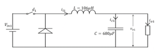 Figure 2: Schematic diagram of the source side buck converter
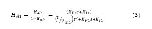
From the control point of view, the buck converter is considered as a power stage (shown in Figure 3), which is controlled by a PI controller. Figure 3 shows the complete control model for the buck converter with specified parameters. The objective is to design a controller to achieve the desired output voltage of 120V from an input supply of 140V. This can be done by controlling the voltage and current flowing through the power stage. Thus, the goal is to design voltage and current controllers (shown in Figure 4). In the diagram, the voltage controller compares the output voltage with the setting voltage V_set1 (120V). Using the droop control governed by droop characteristic shown in Figure 5, the setting value of load current 〖i_l1〗^*can be obtained which is then input to the current controller. The current controller controls an inner loop consisting of a PI controller and the power stage as shown in Figure 6.
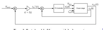 Figure 3: Control model of the source side buck converter
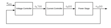 Figure 4: Voltage and current controllers for the source side buck converter
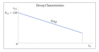 Figure 5: Droop characteristic with a droop gain of 52
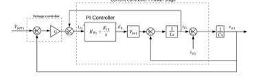 Figure 6: Closed loop current and voltage control scheme for the source side buck converter
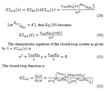
The PI controller parameters include the proportional gain and the integral gain , which need to be determined. For design purposes, the open loop transfer function for the current control is (from Figure 6):
![]() Since the dynamic change in inductor current is faster than that of the voltage across the capacitor, thus can be considered as a disturbance and can be neglected. Then, the modified open loop transfer function becomes
Since the dynamic change in inductor current is faster than that of the voltage across the capacitor, thus can be considered as a disturbance and can be neglected. Then, the modified open loop transfer function becomes
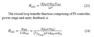
![]() The closed loop transfer function comprising of PI controller, power stage and unity feedback is
The closed loop transfer function comprising of PI controller, power stage and unity feedback is
 3. Stability Analysis of Source Side Converter
The model of the source side buck converter was implemented in Simulink. The stability analysis of the source side buck converter was undertaken in two distinct ways, as described below:
Approach 1: the current loop design
In this approach the current loop is analyzed and the current controller consisting of the power stage and the PI controller is considered. The complete model is shown in Figure 7.
The transfer function of the PI controller is:
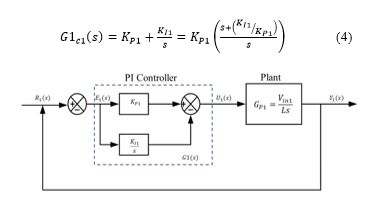 Figure 7: Control system implementation of the source side buck converter
The open-loop transfer function is
Approach 2: voltage and current loop design
In this approach, the entire system including voltage and current controllers is considered. The controller structure as shown in Figure 6 will be considered for the analysis.
The open-loop transfer function system for the design of PI controller is derived from Matlab:
The stability analysis and design of both approaches is performed using Root locus method, Routh Hurwitz criterion, and Nyquist criterion.
3.1. Root Locus Method
The root locus-based design aims to find suitable values for the proportional and integral gains.
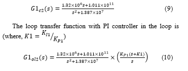
Approach 1: The open-loop transfer function (Equation 6) of the current controller is studied by varying gain . The characteristic equation of (6) is
![]() The resulting root loci of Equation (5) with are shown in Figure 8. From the root loci plot, when gain , the damping ratio is 0.968, which is considered reasonable for the converter. The corresponding value of The characteristic equation has two complex roots (also shown in Figure 8) at:
The resulting root loci of Equation (5) with are shown in Figure 8. From the root loci plot, when gain , the damping ratio is 0.968, which is considered reasonable for the converter. The corresponding value of The characteristic equation has two complex roots (also shown in Figure 8) at:
![]() These are the poles of the closed loop system. Since, these poles are located in the LHP, the closed loop system is stable with reasonable damping.
These are the poles of the closed loop system. Since, these poles are located in the LHP, the closed loop system is stable with reasonable damping.
 Figure 8: Root Loci of equation (11) with ; varies
Approach 2: In this case, similarly, the gain ratio is considered. Equation (10) gives the open-loop transfer function of the system with voltage and current controllers. The root loci of (10) are shown in Figure 9. Clearly, the poles of the closed-loop system are located in the LHP. Thus, the closed loop system is stable.
The closed loop transfer function with is
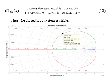 Figure 9: Root Loci of equation (10) with ; varies
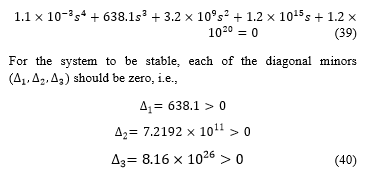
3.2. Routh-Hurwitz Criterion
The Routh-Hurwitz criterion algebraically ascertains the stability requirements for a linear time-invariant (LTI) system modeled with constant coefficients. The criterion tests whether any roots of the characteristic equation lie in the right half s-plane.
Approach 1: The characteristic equation of the closed-loop system is given as and is
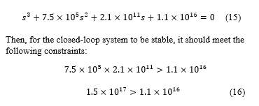
![]() Applying the Routh Hurwitz’s stability criterion to equation (7) yields that the system is stable for and . Thus, the chosen parameter values of stabilize the system.
Applying the Routh Hurwitz’s stability criterion to equation (7) yields that the system is stable for and . Thus, the chosen parameter values of stabilize the system.
Approach 2: The characteristic equation of the closed-loop system is
 The above design satisfies these constraints; hence, the system is stable.
3.3. Nyquist Criterion
The Nyquist criterion graphically reveals information about the number of poles and zeroes of the closed-loop transfer function that are in the right half s-plane. The Nyquist criterion is applied to the two design approaches as follows.
Approach 1: The Nyquist plot of the open loop transfer function (from equation (6)) with is shown in Figure 10, where
 For a minimum phase transfer function, the closed-loop system is stable if there are no encirclements of the critical point From Figure 10, since there are no encirclements of the critical point, thus the closed-loop system is stable. This result is also verified by Matlab.
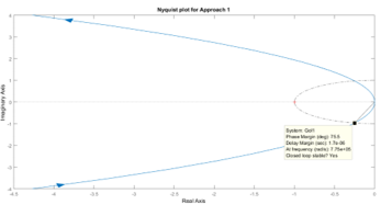 Figure 10: Nyquist plot for Approach 1
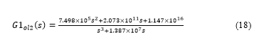
Approach 2: The Nyquist plot of the open loop transfer function (from (10)) with is shown in Figure 11, where the loop transfer function is given as
 From Figure 11, there are no encirclements of the critical point, hence the closed-loop system is stable. This result is also verified by Matlab.
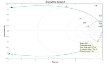 Figure 11: Nyquist plot for Approach 2
Based on the above stability criteria, the values of K_P1 and K_I1 (reported in Table 1 below) stabilize the source side buck converter. The simulation model and corresponding results are shown in appendix and section VII respectively.
Table 1: Values of and for the given source side buck converter
4. Design of CPL
Buck converters can be emulated as instantaneous constant power loads when cascaded with at least one source side DC-DC power converters. For the study, one source side buck converter is considered, and its controller design is proposed in the previous section. Figure 12 shows the control model for a power stage (here buck converter) emulated as CPL.
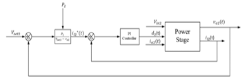 Figure 12: Control Model of CPL
Also, the power stage is supplied with a constant supply of power which characterizes the non-linear nature of the CPL. It thus becomes important to linearize the system about an equilibrium point.
4.1. Linearization of Load Side Converter (CPL)
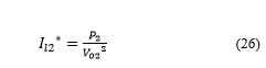
From figure 12 the relationship between setting value of inductor current and incoming voltage of the CPL is non-linear and is given as,
![]() Here, is not considered because the component is added to the simulation model to the closed loop system. Theoretical analysis of the CPL that involves linearization of CPL and its related calculation is based on the open loop circuitry of the CPL which does not have Each of the parameters in Figure 12 can also be represented as the sum of steady state value at equilibrium point and the small signal perturbation around the equilibrium as shown in equation 20.
Here, is not considered because the component is added to the simulation model to the closed loop system. Theoretical analysis of the CPL that involves linearization of CPL and its related calculation is based on the open loop circuitry of the CPL which does not have Each of the parameters in Figure 12 can also be represented as the sum of steady state value at equilibrium point and the small signal perturbation around the equilibrium as shown in equation 20.
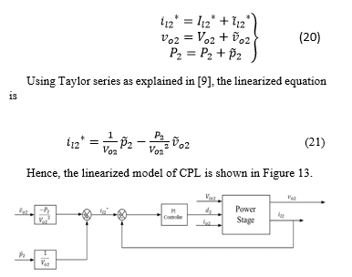 Figure 13: Linearized version of CPL
4.2. PI Control for Linearized CPL (Load Side Buck Converter)
The PI controller parameters namely proportional gain and integral gain need to be determined. The open loop transfer function for the current control is (from Figure 14):
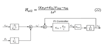 Figure 14: PI control for linearized CPL
Since the dynamic change in inductor current is faster than that of the voltage across the capacitor, thus can be considered as a disturbance and can be neglected. Thus, the modified open loop transfer function becomes
 Equation (24) is the closed loop transfer function of the current controller which is the PI controller and the power stage.
4.3. Power and Bandwidth of CPL
The power stage of the CPL used in this study is the same as that of the source side buck converter. The function of the CPL is to step down the voltage from 120V to 100V. In order to design a PI controller for such a CPL, we have assumed the values of and . This is done, due to two reasons:
- In practical DCMGs, it becomes favorable to have similar current controllers for the source side converter and CPL, as it reduces the complexity of the cascaded network.
- By doing so, the dynamic behavior of both the converters can be compared in order to better understand the working of the CPL.
Thus, .
Since in a CPL, the power supplied is constant, thus Thus, equation (21) is modified and is given as,
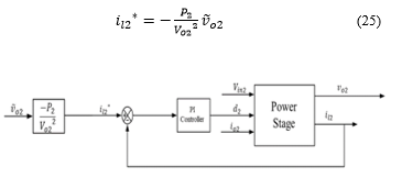 Figure 15: Linearized CPL, ignoring , since
Notice, in Figure 15, the value of the incremental impedance is positive as now the CPL emulates a resistive load, thereby ensuring stability to the DCMG, by keeping its property intact.
Now,
 Since, the parameters of the source side buck converter and that of the CPL is considered the same, thus the droop control of the source side buck converter is analogous to the factor. Thus, assuming and is the desired output voltage of CPL, which is 100V, thus, we get
Using this value of power (derived in Equation (26)), we have done the stability analysis of the CPL to verify that at the CPL is stable.
5. Stability Analysis of CPL (Load Side Converter)
Stability analysis of the Simulink model of the buck converter is similarly done in two distinct ways, as described below:
Approach 1: the current loop design
In this approach the current controller consisting of the power stage and PI controller is considered. The complete model is shown in Figure 16. The transfer function of the PI controller is:
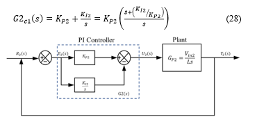 Figure 16: Control system of the CPL
The forward-path transfer function of the feedback control system is
 Approach 2: Current and voltage loop designs
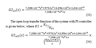
In this approach, the entire system with linearized CPL (having ) and current controller (shown in Figure 15) is considered. The open loop transfer function system with analysis point as the PI controller, is derived from Matlab:
 Three stability analysis criteria are employed toward controller design. These include: The Root Locus method, the Routh Hurwitz criterion and the Nyquist criterion.
5.1. Root Locus Method
The root locus method is aimed to find suitable values for the proportional and integral gains.
Approach 1: Equation (30) gives the open loop transfer function of the current controller with varying gain . The closed-loop characteristic equation for (30) is
 Figure 17: Root Loci of equation (35) with ; varies
The root loci of (30) with are shown in Figure 17. From the root loci, when gain , the damping ratio is 0.897, which is considered reasonable for the converter. Consequently, the value of is selected. The two characteristic equation roots are (shown in Figure 17) are at
 Since these closed-loop poles lie in the LHP, the closed loop system is stable.
Approach 2: In this case, similarly, the design ratio is considered. Equation (34) gives the open loop transfer function of the linearized CPL with the current controller. The root loci of (34) are shown in Figure 18. From the graph, the poles of the closed-loop system lie on the LHP. The closed loop transfer function with is
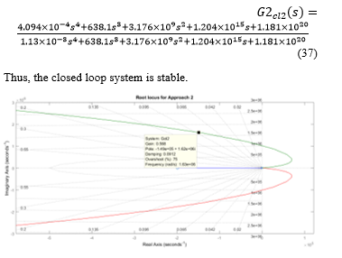 Figure 18: Root Loci of equation (34) with ; varies
5.2. Routh-Hurwitz Criterion
Routh-Hurwitz criterion is similarly applied to determine the conditions for closed-loop stability.
Approach 1: The characteristic equation of the closed-loop system, given as , is
![]() Applying the Routh Hurwitz’s stability criterion to equation (33) yields the result that the system is stable for and . Thus, for the chosen values of , the closed-loop system is stable.
Applying the Routh Hurwitz’s stability criterion to equation (33) yields the result that the system is stable for and . Thus, for the chosen values of , the closed-loop system is stable.
Approach 2: The characteristic equation of the closed-loop system is
 From the conditions in equation (40), it is evident that for the selected parameter values, each of the diagonal minors are greater than 0, thus the closed-loop system is stable.
5.3. Nyquist Criterion
The Nyquist criterion is similarly applied to ascertain the stability of the closed-loop system.
Approach 1: The Nyquist plot of the open loop transfer function (from equation (30)) with is given as
![]() For a minimum phase transfer function, the closed-loop system is stable if there no encirclements of the critical point Since, from Figure 19, there are no encirclements of the critical point, thus the closed loop system is stable. It is also verified by Matlab.
For a minimum phase transfer function, the closed-loop system is stable if there no encirclements of the critical point Since, from Figure 19, there are no encirclements of the critical point, thus the closed loop system is stable. It is also verified by Matlab.
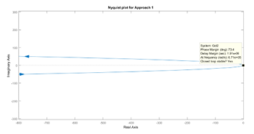 Figure 19: Nyquist plot for Approach 1
Approach 2: The Nyquist plot of the open loop transfer function (from (34)) with is shown in Figure 20, where the loop transfer function is given as
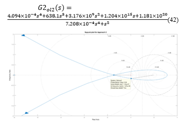 Figure 20: Nyquist plot for Approach 2
The Approach 1 takes into consideration only the current controller and the power stage. The resulting bandwidth of the closed loop transfer function is the bandwidth when the CPL is stable. The values of and are shown below in Table 2. The simulation model of CPL is shown in Appendix and the results are shown in section VII.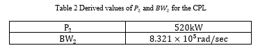
6. Cascaded Network of Source Side Converter and CPL
Cascading two power converters means that the load side converter behaves as the load of the source side converter. In other words, the output voltage of source side converter acts as the input voltage of load side converter, and the output inductor current of source side converter is fed as an input to the load side converter [10].
In our study, we have cascaded the source side buck converter with the linearized CPL. Cascading can be done only when both the power converters are independently stable. In our study, we have shown that the source side buck converter and the CPL are independently stable. Thus, they can be cascaded, thereby forming the smallest DCMG.
In our study, the output voltage of the source side buck converter, is fed as the input voltage to the CPL as . Also, the output inductor current of the source side buck converter, is fed as input current to the CPL, .
Table 3 gives the values of all the parameters of the cascaded power converters, also considered as the smallest DCMG. The simulation model of the cascaded network is shown in Appendix and the results are shown in Sections VII.
Table 3: Values of all the parameters of cascaded source side buck converter and CPL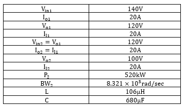
7. Simulation Results of DCMG
The Simulink model for the DCMG is shown in Figure 27 (see Appendix). When the model is simulated, the inductor currents of the source side buck converter and CPL will charge their respective capacitors in order to increase the voltage across the capacitor from 0 to 120V (in case of source buck converter) and from 0 to 100V (in case of CPL). When the load current of 20A is supplied, the voltage across the capacitor decreases slightly, resulting in the inductor current exceeding 20A. The output voltage of 120 V (shown in Figure 21) from the source side buck converter is fed as an input voltage to the CPL. The resulting output voltage of the CPL is 100 V (shown in Figure 23). The output inductor current of 20A (shown in Figure 22) from the source side buck converter is fed as an input current to the CPL. The resulting output inductor current of the CPL also comes out to be 20A (shown in Figure 24). This confirms the cascading of the source side converter with the CPL, to form the smallest DCMG. Clearly, there is no overshoot and no oscillations observed in Figures 21-24.
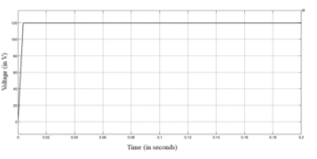 Figure 21: Oscilloscope result of output voltage of source side buck converter
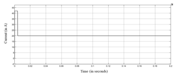 Figure 22: Oscilloscope result of output inductor current of source side buck converter
 Figure 23: Oscilloscope result of output voltage of CPL
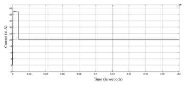 Figure 24: Oscilloscope result of inductor current of CPL
8. Conclusion
This paper discussed the stability analysis of the smallest DCMG that consists of a source side buck converter and a CPL. The cascaded power converters are abundantly found in the DCMGs, and power converters located at the load side that act as CPLs have the potential to cause instability to the entire DCMGs. Thus, it is important to eliminate the instability caused due to CPLs, so that the entire DCMG is stable. Keeping this in mind, the stability analysis of cascaded DC-DC power converters was done. This research proved that despite the presence of CPL, the DCMG can still be made stable. The stability analysis done on the individual components of the cascaded network draws interesting conclusions that support the fact that the DCMG can be stable at certain power level and bandwidth of the CPL controller.
The following are the main results that can be drawn from this research:
- The CPL, that causes instability to the entire DCMG is stabilized at a power level of 520kW and bandwidth of .
- The individual components of the cascaded network, consisting of source side converter and CPL (load side converter) are stable in steady state, thereby making the DCMG stable.
- The DCMG consisting of CPL in cascaded DC-DC power converter network is stable at a certain power level of the load. The power of the load is found out to be 520kW.
- The DCMG consisting of CPL in cascaded DC-DC power converter network is stable with controller bandwidth of , which is the bandwidth of the current controller of the CPL.
It is important to note that the stability analysis of the DCMG with CPL is done with specific parameter values used in this study. The stability analysis can be repeated with a different set of controller design parameters.
Appendix
This paper describes the design and stability analysis of:
- Source side buck converter.
- CPL (emulated as buck converter) and
- Cascaded network of source side buck converter and CPL.
In order to verify that the theoretical results and calculations align well, we have simulated the models using Simulink software. The result of the cascaded network is shown in section VII.
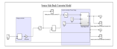 Figure 25: Simulink Model of Source Side Buck Converter
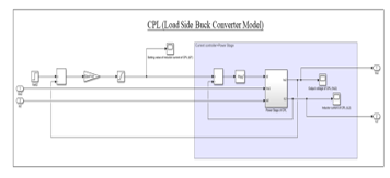 Figure 26: Simulink Model of CPL
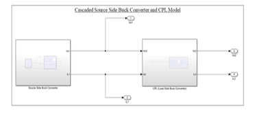 Figure 27: Simulink Model of the cascaded network of source side buck converter and CPL
Conflict of Interest
The authors declare no conflict of interest.
Acknowledgment
The authors are grateful to the Department of Systems Engineering, University of Arkansas, Little Rock, USA for providing necessary facilities to perform the experiments.
- S. Ansari, J. Zhang, K. Iqbal, “Modeling, Stability Analysis and Simulation of Buck Converter in a DC Microgrid,” in 2021 IEEE Kansas Power and Energy Conference (KPEC), 1-4, 2021, doi: 10.1109/KPEC51835.2021.9446255.
- T. Dragičević, X. Lu, J. C. Vasquez, J. M. Guerrero, “DC microgrids— Part I: A review of control strategies and stabilization techniques”, IEEE Trans. Power Electron., 31(7) 4876-4891, 2016, doi: 10.1109/TPEL.2015.2478859.
- D. Olson, “Current market electricity supply issues & trends. It is all about the Peak,” in 2008 IEEE Intl. Telecom. Energy Confer. (INTELEC), 1–5, 2008, doi: 10.1109/INTLEC.2008.4664017.
- S. Luo, “A review of distributed power systems part I: DC distributed power system” IEEE Aerosp. Electron. Syst. Mag. 20(8), 5–16, 2005, doi: 10.1109/MAES.2005.1499272.
- D.K. Fulwani, S. Singh, “Mitigation of Negative Impedance Instabilities in DC Distribution Systems: A Sliding Mode Control Approach”, Springer: Berlin, 2016.
- V. Grigore, J. Hatonen, J. Kyyra, T. Suntio, “Dynamics of a buck converter with a constant power load,” in IEEE Power Electron. Spec. Conf. (PESC 98), vol. 1, 72-78, 1998, doi: 10.1109/PESC.1998.701881.
- M. Srinivasan, “Hierarchical Control of DC Microgrids with Constant Power Loads,” Ph.D. Thesis, The University of Texas, 2017.
- R.W. Erickson and D. Maksimovic, Fundamentals of Power Electronics Norwell, MA: Kluwer, 1997.
- R. Gavagsaz-Ghoachani, L.-M. Saublet, M. Phattanasak, J.-P. Martin, B. Nahid-Mobarakeh, S. Pierfederici, “Active stabilisation design of DC–DC converters with constant power load using a sampled discrete-time model: stability analysis and experimental verification.” IET Power Electronics 11(9), 1519-1528, 2018, doi: 10.1049/iet-pel.2017.0670.
- M. Cupelli, L. Zhu, A. Monti, “Why ideal constant power loads are not the worst case condition from a control standpoint.” IEEE Transactions on Smart Grid 6(6), 2596-2606, 2014, doi: 10.1109/TSG.2014.2361630.