Analysis of Layout Arrangement for CMOS Oscillators to Reduce Overall Variation on Silicon

Adv. Sci. Technol. Eng. Syst. J. 7(5), 46–52 (2022);
 DOI: 10.25046/aj070507
This investigation demonstrates the analysis of various layout arrangements for oscillator (OSC) realized by CMOS technologies. Moreover, the analysis reveals that the serpentine style of OSC stages attains the minimum output variation on silicon. This investigation is firstly verified by post-layout simulations, comparing the variation with different kinds of layout arrangement for OSC designs, including serpentine layout style, straight layout style, and staggered layout style, etc. The proposed design is then realized using 0.18 μm process to justify the performance, where a straight line layout style and a serpentine layout style of OSC are physically fabricated on the same die. Besides, the on-silicon measurement is conducted to give the comparison for these two different styles of OSC designs. The proposed serpentine layout style attains the lowest layout variation when the variations are not homogeneous in different directions on the same silicon plane.
1 Introduction
Thanks to the advancement of CMOS semiconductor technologies, transistors as well as other passive devices are downsized constantly and rapidly. Under the continuous shrinking of nanometer manufacturing process, 180 nm, 90 nm, 40 nm, 28 nm, and even 16 nm, manufacturing variations on wafer become a serious threat to the functionality of logic devices. However, The reason is no matter what process is used, it is suffered from various environmental factors [1]-[14], e.g., voltage, temperature, power surge, process variations, etc. In addition to the environmental factors, the impact of the layout parasitic and arrangement is also an important issue for IC design [15]-[17]. Oscillator (OSC) is one of the major components of digital circuits, which is usually used as the clock generator.
2 Literature Survey
This investigation explores what kind of layout arrangement of OSCs composed of many identical delay stages will attains the best robustness to the variations caused by manufacturing on wafers. The theoretical analysis was verified not only by simulation results, but also physical measurement. In prior works, the measurement results were much worse than the post-layout simulation results mainly due to lack of layout style analysis [18]-[20], and the worst frequency drift is about 0.2 GHz from 1 GHz-3 GHz in these works. Notably, many prior digital circuit design reports never gave details of their clock or OSC generator layout, e.g., [21]-[24]. To keep the simulation conditions consistent for different layout arrangement of OSCs, all OSCs are realized using the same 64 inverters for various 8 × 8 and 1 × 64 combinations in this investigation. Besides, to verify as many possibilities as possible, this investigation demonstrates the analysis of 7 layout arrangements of OSCs by post-layout simulations with full RC extract and Monte Carlo simulation results. Though the layout arrangements look similar for 7 layout arrangements of OSCs, the wiring length between buffers in these cases are not identical. This investigation analytically computes the overall wiring length to predict the RC impact and the variation effect in the different layout styles.
3 Layout Variation Analysis of Oscillator Designs
Figure 1 shows the architecture of a typical differential oscillator. It consists of a Driving Buffer, two 64-to-1 MUX arrays, 64 delay stages, and a Decoder to select the desired frequency. Although
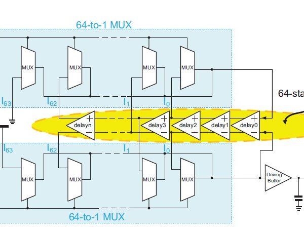
Figure 1: The architecture of the illustrative OSC with 64 delay stages
voltage variation, temperature variation, and process variation are usually considered by chip designers, there are still other variations caused by layout styles. Typical process variation on wafer are usually caused by the non-uniform and linearly degradation doping concentrations of chemical substances. Assume that the variation, PA(0,0), at the origin A(0,0) has the minimum variation c. We then define the variation amount along the x axis for each buffer stage is ”a”, and the variation along y axis is ”b” without the loss of robustness. In other words, the variation is assumed to be a linear function against the distance. And the variation amount is different in different directions on the same die (plane). For example: B(i,j) delay stage has variation PB(i,j) as follows.
PB(i,j) = a · i + b · j + c (1)
- In the case of a straight line arrangement layout of OSC in Figure 2, the total variation Ptotal1(i,j) is found as:
64 1
XX
Ptotal1(i,j)
i=1 j=1
X64 X1 (2)
= (a · i + b · j + c)
i=1 j=1
=2080 · a + 64 · b + 64 · c
Average of variation Ptotalaverage1(i,j) is:
Ptotalaverage1(i,j) = 32.5 · a + b + c (3)
|
|
Figure 2: Straight line layout style of OSC
Notably, buf# (# = 1-64) stands for inverter-based buffers.
- In Figure 3, in the case of a serpentine layout style of OSC, the total variation Ptotal2(i,j) is:
8 8
XX
Ptotal2(i,j)
i=1 j=1
| 8 8
XX = (a · i + b · j + c) i=1 j=1 =288 · a + 288 · b + 64 · c Average of variation Ptotalaverage2(i,j) is: |
(4) |
| Ptotalaverage2(i,j) = 4.5 · a + 4.5 · b + c | (5) |
buf1 buf2 buf3 buf4 buf5 buf6 buf7 buf8 buf16 buf15 buf14 buf13 buf12 buf11 buf10 buf9 buf17 buf18 buf19 buf20 buf21 buf22 buf23 buf24 buf32 buf31 buf30 buf29 buf28 buf27 buf26 buf25 buf33 buf34 buf35 buf36 buf37 buf38 buf39 buf40 buf41 buf42 buf43 buf44 buf45 buf46 buf47 buf48 buf56 buf55 buf54 buf53 buf52 buf51 buf50 buf49 buf57 buf58 buf59 buf60 buf61 buf62 buf63 buf64
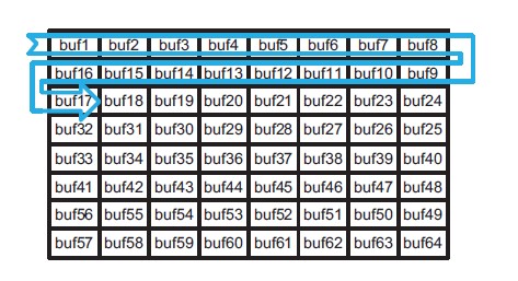
Figure 3: Serpentine layout style of OSC
Based on Eqn. (2) and (4), we make a conclusive derivation as follows.
Ptotal1(i,j) ≥ Ptotal2(i,j)
⇒2080 · a + 64 · b + 64 · c ≥ 288 · a + 288 · b + 64 · c (6)
⇒8 · a ≥ b
Thus, the variation of the serpentine style is better than straight arrangement when ”a” is more than or equal to one eighth of ”b”. This implies that if the variations in different directions are not equal, the serpentine layout style attains the better resistance to overall variations on wafer. This fact was never reported before in any prior work analytically. Notably, the similar analytic approach is applied to other layout styles as those described in the following text.
4 Results and Discussion
4.1 Simulation and Verification
In order to verify as many possibilities as possible before physical realization on silicon, this investigation demonstrates 7 layout arrangements of OSCs as shown in Figure 4, where various arrangements and post-layout simulations with RC extract of OSCs are demonstrated. Given that the central frequency of a 64-stage OSC is 100 MHz by pre-layout simulations, it is assumed that the parasitic variation is ignored. A total of 7 different layout arrangements are shown in Figure 4, namely A, B, C, D, E, F, and G. These styles are briefly described as follows.
- common centroid + even-odd stage interleaved
- common centroid in 2 directions diagonally
- circle to the center
- serpentine
- line by line
- 2-line circle to the center
- straight line
The post-layout simulation of serpentine layout style shows the closest result to 100 MHz. Besides, the error between the serpentine layout style and pre-layout simulation is only 1.9%. In short, the serpentine layout style is the best arrangement proved by this post-layout simulation result.
Because of the limit of chip size and budget, we are only allowed to carry out the serpentine layout style and straight layout style on
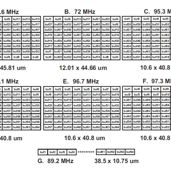
Figure 4: Various arrangements and the clock rates of OSC by post-layout simulations
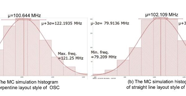
Figure 5: (a) The Monte Carlo simulation histogram of serpentine layout style of OSC; (b) The Monte Carlo simulation histogram of straight line layout style of OSC (MC times=1000)
Table 1: Comparison with prior works.
| MWCL[21] | VLSI[22] | JSSC[23] | JSSC[24] | this work | ||
| Year | 2017 | 2019 | 2019 | 2021 | 2022 | |
| VDD (V) | 1 | 0.8 | 1.2 | 1 | 3.3 | |
| Layout arrangement | straight | straight | straight | straight | serpentine | straight |
| Layout variation | N/A | N/A | N/A | N/A | Yes | |
| Accuracy | N/A | N/A | N/A | N/A | 95.5% | 88.7% |
| Frequency range | 1 MHz | 3.2 GHz-4 GHz | 2.1 GHz-3.1 GHz | 3.6 GHz-3.6175 GHz | 20 MHz-180 MHz | |
| Bandwidth | 10 MHz | 10 MHz | 10 MHz | 100 MHz | 100 MHz | |
| Adjustable frequency | Yes | Yes | Yes | Yes | Yes | |
| Chip Area (mm2) | 0.75 | 1 | 0.25 | 0.00525 | 1.3 | |
| Chip Area
(Normalization) (10−4 mm2) |
1.775 | 2.36 | 0.6 | 0.108 | 0.4 | |
| FOM | 8.8 | 2820 | 11888 | 15700 | 12100, 23606∆ | |
FOM = VDDFrequency range· Normalized Chip Area· Bandwidth
∆ This FOM is counted only by the area of the serpentine style.
silicon. Their areas are 10.6 × 40.8 µm2 (serpentine) and 38.5 × 10.75 µm2 (straight line), respectively. Figure 5 shows the Monte Carlo simulation results of two different layout styles to verify the reliability, respectively. As shown in Figure 5, the central frequency of serpentine layout style is closer to 100 MHz, which is set to be the central frequency of this investigation.
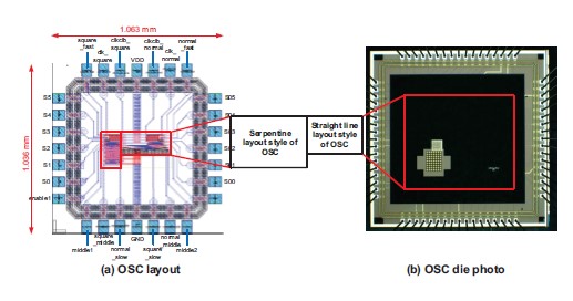
Figure 6: (a) OSC layout; (b) OSC die photo
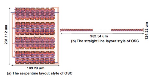
Figure 7: The enlarged layout style of OSC (a) serpentine style; (b) straight line style
4.2 Measurement and Performance Comparison
To verify the previous analysis, the proposed OSC designs are realized using TSMC 180 nm CMOS process. The layout and die photo of the OSCs are shown in Figure 6 (a) and (b), respectively, where the total chip area is 1.063 × 1.063 mm2, and the core area is 989 × 344 µm2. Notably, there are 2 OSC designs (straight line, serpentine) on the same die. The detailed layouts of the mentioned OSCs are enlarged in Figure 7. To highlight the influences from the different layout styles, the space between any two adjacent stages in Figure 7 is the same. The chip measurement setup is shown in Figure 8. The chip is soldered on the PCB to reduce noise interference. The Agilent E3631A Power Supply provides the required voltages and enable signals to the chip. Arbitrary waveform generator Agilent 33522A provide the 6-bit selection code. The oscilloscope WaveRunner610Zi is used to observe waveforms and monitor the circuit operations.
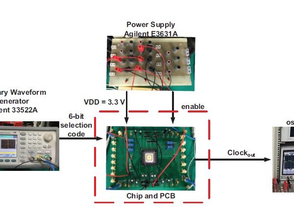
Figure 8: Measurement setup and equipment
95.5 MHz
| buf1 | buf2 | buf3 | buf4 | buf5 | buf6 | buf7 | buf8 |
| buf16 | buf15 | buf14 | buf13 | buf12 | buf11 | buf10 | buf9 |
| buf17 | buf18 | buf19 | buf20 | buf21 | buf22 | buf23 | buf24 |
| buf32 | buf31 | buf30 | buf29 | buf28 | buf27 | buf26 | buf25 |
| buf33 | buf34 | buf35 | buf36 | buf37 | buf38 | buf39 | buf40 |
| buf41 | buf42 | buf43 | buf44 | buf45 | buf46 | buf47 | buf48 |
| buf56 | buf55 | buf54 | buf53 | buf52 | buf51 | buf50 | buf49 |
| buf57 | buf58 | buf59 | buf60 | buf61 | buf62 | buf63 | buf64 |
10.6 x 40.8 um
- The block diagram ofserpentine layout style of OSC
|
|
88.7 MHz 38.5 x 10.75 um
- The block diagram of straightline layout style of OSC
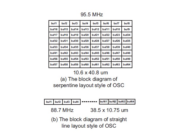
Figure 9: (a) The block diagram of serpentine layout style of OSC; (b) The block diagram of straight line layout style of OSC
Figure 9 shows the block diagrams of serpentine layout style and straight line layout style of OSCs in Figure 6 and 7. Figure 10 (a), (b) show the measurement waveforms of these 2 layout styles, respectively. By comparing the pre-layout simulation (100 MHz) with the measurement results, the deviations of serpentine layout style and straight line layout style of OSCs are 4.5% and 11.3%, respectively.
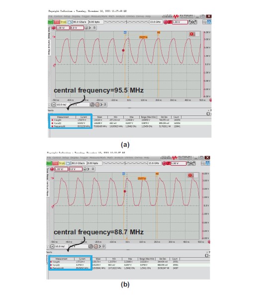
Figure 10: (a) The measurement waveform of central frequency of serpentine layout style; (b) The measurement waveform of central frequency of straight layout style
To verify the selectability of OSCs, Figure 11 shows the comparison of pre-layout simulation, post-layout simulation, and the chip measurement results by different selection codes (1-15). The
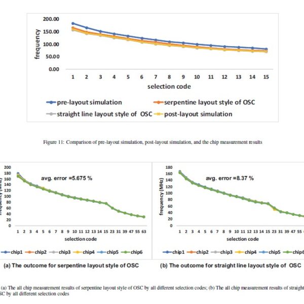
style of OSC by all different selection codes
measurement result of the serpentine layout style is closer to the prediction of post-layout simulations. To justify the repeatability of the chip measurement, all 6 chips are measured with 10 times and the results are shown in Figure 12. The average error of the serpentine style layout is smaller than that of the straight line counterpart. Table 1 tabulates the performance comparison of the proposed design and several recent works about layout arrangement. The proposed design achieves the second best FOM because our chip contains two layout arrangements of OSCs. In other words, the chip consumes much larger area than others. Notably, the proposed design would have the best FOM if only the area of the serpentine style is accounted for. The FOM will become 23606, simply the best of all.
5 Future Enhancement
The proposed OSC is a prototype for verifying the layout arrangement impact on CMOS oscillators. Thus, the main issue to be improved in the future is to enlarge the frequency range.
6 Conclusion
This investigation presents detailed analysis of OSC layout styles to conclude that the serpentine layout significantly reduces the variation impact. Moreover, the proposed layout method can be used to other CMOS processes. The proposed serpentine layout style can be applied in other CMOS technology nodes to make the chip performance more predictable in the early design stage.
7 Acknowledgment
This work was partially supported by FocalTech Systems Co., Ltd,
Taiwan, under grant NO. N109130. The authors would like to express their deepest gratefulness to TSRI (Taiwan Semiconductor Research Institute), Taiwan, for their chip fabrication service.
- Z. Abbas, A. Zahra, M. Olivieri, and A. Mastrandrea ”Geometry scaling impact on leakage currents in FinFET standard cells based on a logic-level leakage estimation technique,” Microelectronics, Electromagnetics and Telecommuni- cations, 521(4), 283-294, 2018, doi:10.1007/978-981-10-7329-8 29.
- S.-K. Shin, W. Yu, Y.-H. Jun, J.-W. Kim, B.-S. Kong, and C.-G. Lee, ”Slew-rate-controlled output driver having constant transition time over pro- cess, voltage, temperature, and output load variations,” IEEE Trans. on Circuits and Systems II: Express Briefs (TCAS-II), 54(7), 601-605, 2007, doi:10.1109/TCSII.2007.895314.
- R.-C. Kuo, H.-Y. Tseng, J.-W. Liu, and C.-C. Wang, ”On-chip process and tem- perature compensation and self-adjusting slew rate control for output buffer,” in Asia Pacific Conf. on Postgraduate Research in Microelectronics Electronics (PrimeAsia), 37-40, 2011, doi:10.1109/PrimeAsia.2011.6075065.
- T.-J. Lee, W. Lin, and C.-C. Wang, ”Slew rate improved 2 VDD output buffer using leakage and delay compensation,” in IEEE Inter. Conf. on Electron Devices and Solid-State Circuits (EDSSC), 1-2, 2014, doi:10.1109/EDSSC.2014.7061267.
- C.-L. Chen, H.-Y. Tseng, R.-C. Kuo, and C.-C. Wang, ”On-chip MOS PVT variation monitor for slew rate self-adjusting 2 VDD output buffers,” in IEEE Inter. Conf. on IC Design Technology (ICICDT), 1-4, 2012, doi:10.1109/ICICDT.2012.6232876.
- C.-L. Chen, H.-Y. Tseng, R.-C. Kuo, and C.-C. Wang, ”A slew rate self- adjusting 2 VDD output buffer with PVT compensation,” in IEEE VLSI Design, Automation and Test (VLSI-DAT), 1-4, 2012, doi:10.1109/VLSI- DAT.2012.6212590.
- C.-C. Wang, C.-L. Chen, R.-C. Kuo, H.-Y. Tseng, J.-W. Liu, C.-Y. Juan, ”On- chip process and temperature monitor for self-adjusting slew rate control of 2 VDD output buffers,” IEEE Trans. on Circuits and Systems I: Regular Papers (TCAS-I), 60(6), 1432-1440, 2013, doi:10.1109/TCSI.2012.2226515.
- T.-J. Lee, K.-W. Ruan, and C.-C. Wang, ”32% slew rate and 27% data rate improved 2 VDD output buffer using PVTL compensation,” in IEEE Inter. Conf. on IC Design Technology (ICICDT), 1-4, 2014, doi:10.1109/ICICDT.2014.6838601.
- C.-C. Wang, T.-Y. Tsai, T.-J. Lee, and K.-W. Ruan, ”2 VDD output buffer with 36.4% slew rate improvement using leakage current compensation,” Electronics Letters (EL), 53(2), 62-64, 2017, doi:10.1049/el.2016.2351.
- C.-C. Wang, T.-Y. Tsai, and W. Lin, ”A 90-nm CMOS 800 MHz 2 VDD output buffer with leakage detection and output current self-adjustment,” Ana- log Integrated Circuits and Signal Processing (AICSP), 97(2), 343-350, 2018, doi:10.1007/s10470-018-1285-3.
- D. R. Dancer, “Digitally controlled ring oscillator,” U.S.A. Patent US96112503, 2006.
- S. Wadhwa, D. Mehrotra, and P. M. Furth, “Low voltage, wide frequency range oscillator,” U.S.A. Patent US8975974B2, 2012.
- C. L. Lin, “Quadrature output ring oscillator and method thereof,” R.O.C. Patent TW 1547095 B, 2015.
- M. More and P. Apte, ”Digitally controlled oscillator with variable capacitive loading,” in International Conference on Communication and Signal Process- ing (ICCSP), 1723-1726, 2016, doi:10.1109/ICCSP.2016.7754460.
- Y. Wang, L. Zhang, T. Liu, Y. Wang, R. Hu, D.-B. Fu, and G.-B. Chen, ”Layout design of metal-insulator-metal capacitor array for reducing parasitic influ- ences,” in 2016 IEEE International Nanoelectronics Conference (INEC), 1-2, 2016, doi:10.1109/INEC.2016.7589265.
- Y. S. Hristov, S. D. Kostadinov, D. G. Gaydazhiev, and I. S. Uzunov, ”Influence of the layout parasitic effects on the performance of current mode amplifier de- signed using 32nm CMOS technology,” in 2018 IEEE XXVII International Sci- entific Conference Electronics (ET), 1-4, 2018, doi: 10.1109/ET.2018.8549671.
- M. Hifumi, H. Maruoka, S. Umehara, K. Yamada, J. Furuta, and K. Kobayashi, ”Influence of layout structures to soft errors caused by higher-energy particles on 28/65 nm FDSOI flip-flops,” in 2017 IEEE International Reliability Physics Symposium (IRPS), 5.1-5.4, 2017, doi:10.1109/IRPS.2017.7936406.
- B. Likhterov and A. Belenky, ”Traveling-wave ring oscillator — a new archi- tecture for a transmission line based oscillator,” in 2016 IEEE International Conference on the Science of Electrical Engineering (ICSEE), 1-5, 2016, doi:10.1109/ICSEE.2016.7806048.
- B. Likhterov and A. Belenky, ”Traveling-wave ring oscillator – simulations and prototype measurements for a new architecture for a transmission Line Based oscillator,” in 2018 IEEE International Conference on the Science of Electrical Engineering in Israel (ICSEE), 1-5, 2018, doi:10.1109/ICSEE.2018.8645996.
- D. Garinto, A. Syahriar and S. Budiyanto, ”A novel op-Amp based LC oscillator for wireless communications,” in IECON 2020 The 46th Annual Conference of the IEEE Industrial Electronics Society, 2243-2248, 2020, doi:10.1109/ICSEE.2018.8645996.
- A. Mahmoud, P. Andreani and F. Pepe, ”A 2.8–3.8-GHz low-spur DTC- based DPLL with a class-D DCO in 65-nm CMOS,” IEEE Microwave and Wireless Components Letters (MWCL), 27(11), 1010-1012, 2017, doi: 10.1109/LMWC.2017.2750089.
- I. Taha and M. Mirhassani, ”A 24-GHz DCO with high-amplitude stabiliza- tion and enhanced startup time for automotive radar,” IEEE Transactions on Very Large Scale Integration (VLSI) Systems, 27(10), 2260-2271, 2019, doi:10.1109/TVLSI.2019.2924018.
- H. Liuet, Z. Sun, H. Huang, W. Deng, T. Siriburanon, J. Pang, Y. Wang, R. Wu,
T. Somey, A. Shirane, and K. Okada, “A 265µW fractional-N digital PLL with seamlessautomatic switching subsampling/sampling feedback path and duty- cycled frequency-locked loop in 65nm CMOS,” IEEE Journal of Solid-State Circuits (JSSC), 54(12), 3478–3492, 2019, doi:10.1109/JSSC.2019.2936967. - S. Kundu, L. Chai, K. Chandrashekar, S. Pellerano, and B. R. Carlton, ”A self-calibrated 2-bit time-period comparator-Based Synthesized Fractional-N MDLL in 22-nm FinFET CMOS,” IEEE Journal of Solid-State Circuits (JSSC), 56(1), 43-54, 2021, doi:10.1109/JSSC.2020.3021279.