S-Parameters Optimization in both Segmented and Unsegmented Insulated TSV upto 40GHz Frequency

Adv. Sci. Technol. Eng. Syst. J. 2(3), 268–276 (2017);
 DOI: 10.25046/aj020336
Segmented and unsegmented 3D insulated copper through silicon vias (TSVs) of diameter 10 micro-meter, height 100 micro-meter and silicon of sizes 100 micro-meter by 100 micro-meter by 100 micro-meter are modeled using analysis system (ANSYS), equivalent circuit using advanced design system (ADS) at frequency ranges between 100MHz and 40GHz and 10MHz step size. The segmented via is divided into three parts. Each part modeled separately. Scattering parameters are found. The outputs are optimized to give accurate results. The results show that the outputs reflect the transmission characteristics of an ideal TSV.
1. Introduction
S-Parameters Optimization in both Segmented and Unsegmented Insulated TSV was featured in [1]. This paper advances the work done in [1] by optimizing the S-Parameters but to a higher frequency of 40GHz. S parameters have been given much considerations since they allow a device to be treated as a black box with inputs and resulting outputs, making it possible to model a system without having to deal with the complex details of its actual structure.
In the previous paper [1], the scattering parameters especially the S21 which defines power loss in TSVs was given much attention. Here we consider other parameters such as S11 too.However, the bandwidth of todays Integrated Circuits (IC’s) keeps increasing. This paper has found it important to characterize their performance over wide frequency ranges up-to a maximum of 40GHz. This is because the traditional low-frequency parameters such as resistance, capacitance, and gain can be frequency dependent and therefore may not fully describe the performance of the IC at the desired frequency. Moreover, it may not be possible to characterize every parameter of a complex IC over frequency therefore system-level characterization using S-parameters may provide better and more reliable data [2, 3, 4].
2. S-Parameters
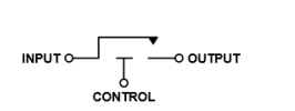
A simple RF relay is used to demonstrate the techniques of high-frequency model verification.It is considered a three-port device with an input, output and a control to switch the circuit on and off. However, since the device performance is independent of the control terminal it is simplified to a two-port device. Therefore, it is characterized by observing the behavior at its input and output terminals. This is elaborated in figure 1.
Where, a1 = incident wave on port 1 b1 = reflected wave from port 1 a2=incidentwaveonport2(reflectedfromtheload)
b2 = reflected wave from port 2
ZS= source impedance ZL= load impedance
From figure 2 notations, S-parameters defined the reflected waves b1 and b2 as shown in equation (1) and (2)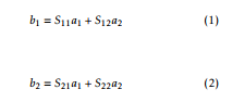
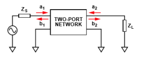
If ZS = Z0, that is; impedance of two-port input, no reflections occur and a1 = 0. If ZL = Z0 that is; the impedance of two-port output, no reflections occur and a2 = 0. Therefore we can define the S-parameters, based on the matched condition as follows: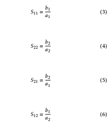
To realize the above parameters in a physical system, ZS, Z0, and ZL must be matched. For most systems this is easily implemented over a wide frequency range [2]. The authors implemented up to a maximum frequency of 40GHz.
3 Through Silicon Via (TSV) Technology
This study contributes to knowledge about parameter distribution, transmission properties, electrical effects and so on. This is the basic foundation of 3D IC [5, 6].
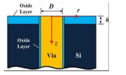
Figure 3 shows a structure of a TSV. It’s made up of key areas such as via where the filler material is put. The filler material is copper in most cases since it’s a good conductor. The letter z defines the via depth direction, D is the via diameter while r is the via radius direction. The TSV is surrounded by an oxide layer which is silicon dioxide and h defines its height or thickness. The whole model is done in silicon which is a substrate material. Increasing power, performance and financial bottle-necks beyond 3222 nm industry has led to development of TSV [8]. TSVs can be processed in different ways. For instance; Front
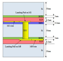
End Of Line (FEOL), Back End Of Line (BEOL), Via First (poly-silicon filled via) whereby TSVs are fabricated before transistors. Via Middle (copper filled via) whereby TSVs are fabricated before the copper interconnects and Via Last (copper liner) where TSVs are fabricated after bonding the stack. Figures 4 and 5 show the differences between via first and via last technologies. Potential reliability issues can arise due to during or after these processes. During the via design the stress management can be a problem. This is experienced through via fabrication which may induce tensile stresses in silicon, via may also experience compressive hoop stresses which could lead to via buckling, the quantity and spacing of via may also result in undesirable stress fields and finally the most common thermally induced stresses due to coefficient of Thermal Expansion (CTE) mismatch which may lead to cracking of the silicon wafer. Thermal management is another design problem. This is due to large and non-uniform heat flow within the package. There also exists redundancy in the design used.
Apart from the problems experienced during design of TSVs, some problems are experienced during processing. These include; metal voiding which happens during material filling, uniform via wall material deposition, active Integrated Circuit (IC) surface connectivity and wafer handling problem. Other challenges are experienced during the performance of the TSVs. For instance; limited reliability, thermal cycling, electro migration, silicon depletion at or around the via and also shock and vibration. Noise coupling, fabrication process limits and failure issues have been discussed in [10]. However TSV has several advantages such as reducing the delay, power and area. It also promotes the integration of heterogeneous devices.
4 TSV Liner
Although the TSV has several advantages, these would not be viable unless the TSV is well protected. This is enhanced by TSV liner. In our paper we propose the use of silicon dioxide material as a liner due to its many advantages. Dielectric liner functions as electrical isolation between the TSV metal fill and silicon substrate; therefore it should have zero leakage, high breakdown voltage, low stress, process temperature compatibility, good step coverage and uniformity. Silicon dioxide has these properties. However, other materials such as nitride and polymers are also used as liners for TSV applications [11,12, 13].
5 Methodology
There are several ways of characterizing the ports behavior. One is by admittance matrix Y or impedance matrix Z which defines the relationship between voltages and currents at the ports [14]. Various ways are available and are used to calculate functions that can accurately produce port characteristics within a desired frequency at the same time meet the physical requirements such as symmetry, causality, stability and passivity [15,16, 17 and 18]. The second way of characterizing the port behavior is by use of the incident and reflected waves that are related through the scattering parameter matrix [14], [19], [20]. This second way is often applicable in high speed electronics modeling over the admittance formulation because it gives more accurate results at very high frequencies; it is also useful in applying pure transfer functions models in a simulation. These transfer function capability provides an easy way of observing internal voltages and currents in a subnetwork represented by a Y-, Zor S-parameter-based port equivalent, and it reduces the computational burden of the model identification process as the number of ports is reduced [14].
As discussed in, [14], Y parameter models can be interfaced with electromagnetic transients program tools through equivalent circuits [21], [22]. However, the circuit experiences inaccuracy hence should be avoided and instead the model can be represented using convolutions [23], [24] which are considered a little bit standard as per [25, 26]. This paper is accessing the variation of S-parameters on a single insulated unsegmented TSV and segmented TSV over a frequency range of 40GHz. The S21 parameter which represents the insertion loss is the key area of research. Insertion loss is expected to be as low as possible on the graphs. The equivalent circuits of the unsegmented and segmented vias are simulated and the results represent the TSV characteristics. The segmented TSV gave a much lower insertion loss as compared to the unsegmented one. This shows that its more reliable and can be used to alleviate the insertion loss problem mainly experienced in the TSV thereby alleviating that reliability problem in 3D packages. The S parameters are converted to Z parameters, Z21 which gave much lower values than the S21 but still maintained the TSV characteristics. S11 characteristics are also listed.
5.1 Unsegmented TSV
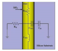
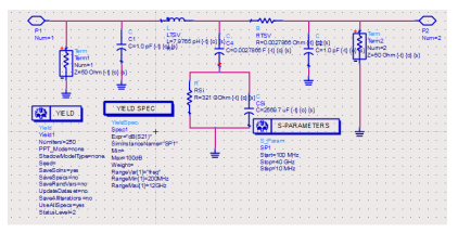
Figure 6 represents a vertical TSV model. The RTSV , CTSV and LTSV represent resistance, capacitance and inductance respectively along the TSV. RSi and CSi are the resistance and capacitance respectively in the silicon substrate.
The Advanced Design System (ADS) simulator developed the schematic in figure 7 from the model in figure 6. LTSV, RTSV and C4 are inductance, resistance and capacitance respectively along the TSV. The C1 and C2 are capacitances in the TSV liner, RSi and CSi are the resistance and capacitance respectively along the silicon substrate, S parameter with the terms give the insertion and other loses experienced in TSV while the yield ensures accurate results are obtained. The schematic is an improvement of the work done in [1, 6]. In [6], silicon dioxide layer which act as a TSV liner was not included in the circuit. Moreover, optimization was not done to enhance accurate results. This has been done in this paper by including the yield in the system the frequency has been extended to 40GHz too. A total of 250 trials were made to finally end up with 100 percent yield. The trials were done within the frequency ranges specified in the S-parameter icon. S11 parameters have also been discussed.
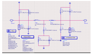
5.2 Segmented TSV
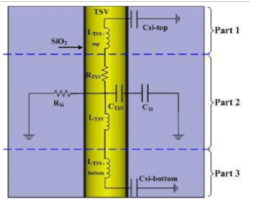
Figure 8 represents a partitioned vertical TSV. It is divided into three main parts namely; Part 1, Part 2 and Part 3. The partitioning of the TSV reduces the insertion loss which is a reliability problem in TSVs. Parasitic resistance, inductance and capacitance exists just like in figure 6.
lator layer silicon dioxide. The LTSV, RTSV and C4 are the inductance, resistance and capacitance respectively along the TSV. RSi and CSi are the resistance and capacitance respectively along the silicon substrate. The S-parameter and the yield simulators play the same role as in figure 7.
6 Results and Discussions
6.1 Unsegmented TSV
Figure 10 looks exactly as what was done in [1] but the difference is that the frequency range has been stretched to 40GHz. The dB values are decreasing with the increased frequency. The markers, m3 and m4 define the dB values at those particular frequencies.
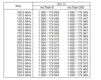
Figure 11 is a list of S11 parameters with varying frequencies. As the frequency increases the S11 value decreased as evident in the list.
6.2 Segmented TSV
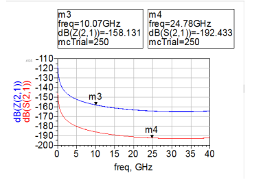
Figure 12 describes the dB(S(2,1)) with variation in frequency up to 40GHz. The m3 and m4 in this figure defined the parameter at those frequencies. However, the maximum power on the ’YIELD SPEC’ was varied to enhance smooth curve; dB(Z(2,1)) was not plotted too, although the graph gave exactly the variations discussed in [1].
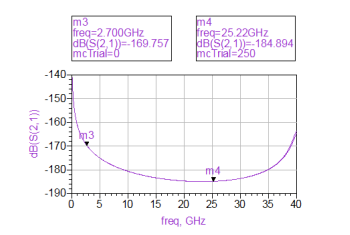
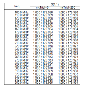
Figure 13 on the other hand described S11 parameter with varying frequencies. It was noted that just like in the unsegmented TSV, the S11 values decreased with increased frequencies, the differences in S11 are however slight. However, The S11 in the segmented TSV is slightly higher than that in unsegmented one at the same frequency.
7 Conclusions and Recommendations
Both segmented and unsegmented TSV were modeled using ADS software. This work was an improvement of work done by [1 and 6]. In the previous work [1], the maximum frequency range considered was 20GHZ but in this paper, it has been stretched to 40GHz. We recommend extension of the frequency range because by doing so, its application will be possible on more electronic devices made. Optimization of the values also promotes more accurate results. Just like in the previous work we intend to do the modeling of TSV in more portions rather than three parts in future. We will also include the effects of changes in length and thickness of the TSV alongside use of other TSV liner materials such as polymers on the power losses. With more factors put into consideration, we hope to reduce the insertion losses in TSV even further. There has been increasing need of cheaper and high performance devices in the world today. These have made researches seek for solutions to these problems. Figure 14

describes the future of TSVs. Variation of TSV pitch have greatly influenced the cost and performance of TSV which later influence the devices made between the year 2006 and the current 2017. In the year 2006, the cost of manufacturing TSVs was too high yet the performance of the devices made from the technology was poor due to high TSV pitch. This reduced the reliability of the electronic devices made
[1].
Just like in [1],as years went by, research was done and the researchers realized that the TSV pitch size greatly influenced the cost and performance of the TSV modeled devices. They therefore proposed the reduction of the TSV pitch from 100 micro-meters in the year 2006 to less than 1 micro-meter now; 2017. Through the gradual reduction in the TSV pitch size, the cost of production has gone down and the performance of the electronic devices made from the TSV technology has increased. High costs and low performance was evident in 2D conventional designs. However, the use of semiconductors, MEMS, RF devices and polymer devices enhanced development of partially
3D dedicated design to fully 3D dedicated designs which experience low costs and high performance.
Acknowledgment The first author would like to acknowledge the enthusiastic supervision of Prof. HE Song Bai and Zhang Xuliang for their great guidance and advice throughout this paper; they truly inspired me. Their will to motivate me played a major role in this paper. I would also like to thank them for giving me some good examples of some published papers which are related to this work. I would not forget to thank University of Electronic Science and Technology of China (UESTC) for providing a conducive environment and materials to work with on our paper. Our appreciations also go to the laboratory technicians and members who were patient with us all the time. They also contributed to some great ideas in this paper. Finally, we would not like to forget our families and friends for their understanding and support in our work without which this work would not be possible.
- J. M. Atieno, X. Zhang and H. S. Bai, ”Sparameters optimization in both segmented and unsegmented insulated TSV,” 2016 International Conference on Integrated Circuits and Microsystems (ICICM), Chengdu, 228–232, 2016.
- Joseph Creech, ”S-Parameters Allow HighFrequency Verification of RF Switch Models” Analog Dialogue, 45(10), 1 4, 2011.
- Paul, TDR: taking the pulse of signal integrity. EDN, September 3, 2007.
- Bowick, Chris, John Blyler and Cheryl Ajluni, ”RF Circuit Design” Newnes, 2007.
- W. R. Davis et al., ”Demystifying 3D ICs: the pros and cons of going vertical,” in IEEE Design and Test of Computers, 22(6), 498–510, Nov.- Dec. 2005.
- Z. Ma, Z. Yan, Y. Xiong, M. Zhang and G. Shi, ”A novel segmented equivalent circuit modeling method of TSV in 3D IC,” 2013 5th IEEE International Symposium on Microwave, Antenna, Propagation and EMC Technologies for Wireless Communications, Chengdu,646–649, 2013.
- S. K. Ryu, K. H. Lu, T. Jiang, J. H. Im, R. Huang and P. S. Ho, ”Effect of Thermal Stresses on Carrier Mobility and Keep-Out Zone Around Through-Silicon Vias for 3-D Integration,” in IEEE Transactions on Device and Materials Reliability, 12(2) 255–262, June 2012.
- D. Z. Pan et al., ”Design for manufacturability and reliability for TSV-based 3D ICs,” 17th Asia and South Pacific Design Automation Conference, Sydney, 750–755, NSW,2012.
- J. Pak, M. Pathak, S. K. Lim and D. Z. Pan, ”Modeling of electromigration in through-silicon-via based 3D IC,” 2011 IEEE 61st Electronic Components and Technology Conference (ECTC), Lake Buena Vista, FL, 1420–1427, 2011.
- J. Lim et al., ”Shielding structures for through silicon via (TSV) to active circuit noise coupling in 3D IC,” 2015 10th International Workshop on the Electromagnetic Compatibility of Integrated Circuits (EMC Compo), Edinburgh, 248–251, 2015.
- S. Ramaswami et al., ”Process Integration Considerations for 300 mm TSV Manufacturing,” in IEEE Transactions on Device and Materials Reliability, 9(4), 524–528, Dec. 2009.
- L. Zhang, H. Y. Li, S. Gao and C. S. Tan, ”Achieving Stable Through-Silicon Via (TSV) Capacitance with Oxide Fixed Charge,” in IEEE Electron Device Letters, 32(5) 668–670, May 2011.
- Q. Chen, C. Huang, Z. Tan and Z. Wang, ”Low Capacitance Through-Silicon-Vias With Uniform Benzocyclobutene Insulation Layers,” in IEEE Transactions on Components, Packaging and Manufacturing Technology, 3(5) 724–731, May 2013.
- B. Gustavsen and H. M. J. De Silva, ”Inclusion of Rational Models in an Electromagnetic Transients Program: Y Parameters, Z-Parameters, SParameters, Transfer Functions,” in IEEE Transactions on Power Delivery, 28(2), 1164–1174, April 2013.
- B. Gustavsen and A. Semlyen, ”Rational approximation of frequency domain responses by vector fitting,” in IEEE Transactions on Power Delivery, 14(3), 1052–1061, Jul 1999.
- B. Gustavsen, ”Improving the pole relocating properties of vector fitting,” in IEEE Transactions on Power Delivery, 21(3), 1587–1592, July 2006.
- D. Deschrijver, M. Mrozowski, T. Dhaene and D. De Zutter, ”Macromodeling of Multiport Systems Using a Fast Implementation of the Vector Fitting Method,” in IEEE Microwave and Wireless Components Letters, 18(6), 383 385, June 2008.
- P. Triverio, S. Grivet-Talocia, M. S. Nakhla, F. G. Canavero and R. Achar, ”Stability, Causality, and Passivity in Electrical Interconnect Models,” in IEEE Transactions on Advanced Packaging, 30(4), 795–808, Nov. 2007.
- K. Kurokawa, ”Power Waves and the Scattering Matrix,” in IEEE Transactions on Microwave Theory and Techniques, 13(2), 194–202, Mar 1965.
- Z. Zhongyuan, L. Fangcheng and L. Guishu, ”A High-Frequency Circuit Model of a Potential Transformer for the Very Fast Transient Simulation in GIS,” in IEEE Transactions on Power Delivery, 23(4), 1995 1999, Oct. 2008.
- A. S. Morched, J. H. Ottevangers and L. Marti, ”Multi-port frequency dependent network equivalents for the EMTP,” in IEEE Transactions on Power Delivery, 8(3), 1402–1412, July 1993.
- B. Gustavsen, ”Computer code for rational approximation of frequency dependent admittance matrices,” in IEEE Transactions on Power Delivery, 17(4), 1093–1098, Oct 2002.
- T. Noda, ”Identification of a multiphase network equivalent for electromagnetic transient calculations using partitioned frequency response,” in IEEE Transactions on Power Delivery, 20(2), 1134–1142, April 2005.
- C. Dufour, J. Mahseredjian and J. Belanger, ”A Combined State-Space Nodal Method for the Simulation of Power System Transients,” in IEEE Transactions on Power Delivery, 26(2), 928–935, April 2011.
- A. Semlyen and A. Dabuleanu, ”Fast and accurate switching transient calculations on transmission lines with ground return using recursive convolutions,” in IEEE Transactions on Power Apparatus and Systems, 94(2), 561–571, Mar 1975.
- M. Motoyoshi, ”Through-Silicon Via (TSV),” in Proceedings of the IEEE, 97(1), 43–48, Jan. 2009.