A Novel Pulse Position Modulator for Compressive Data Acquisition

Adv. Sci. Technol. Eng. Syst. J. 4(1), 171–182 (2019);
 DOI: 10.25046/aj040117
This work extends the development of the nonuniform Parallel Digital Ramp Pulse Position Modulation Analog-to-Digital Converter (PDRADC) architecture. The continuous to discrete transform of the PDRADC is achieved by partitioning the signal amplitude axis into P nonoverlapping partitions that sample the analog input at input signal driven instances. Each partition contains L uniform levels with different quantization step sizes such that the dynamic range of the partitions are related as a geometric series. It is shown that this new architecture satisfies the Nyquist requirement on average (Beutler’s condition) and results in a random additive sampling architecture that is alias free (Shapiro- Silverman condition). Additionally, it is shown that the geometric partitioning causes the signal-to-quantization noise ratio (SQNR) to remain approximately constant. A comprehensive design paradigm is presented, including circuits to affect the desired response, the format of the encoded digital samples and the corresponding transformation to determine the equivalent analog voltage. Lastly, although the thrust of this paper is not reconstruction techniques, reconstruction is, nevertheless, compulsory, and recovery and reconstruction is demonstrated through simulations.
1. Introduction
This communication is an extension of work originally presented at a conference on Electrical and Computer Engineering [1] and this current paper significantly expands upon the initial concept proposed in the orig- inal material. Although the most common form of sampling is uniform sampling, there are many cases where nonuniform sampling arises and is intentional [2]. Compressed Sensing (CS) ,[3, 4], is based upon, and operates on nonuniform samples. In CS, the goal is to compress at the time of sampling [5]. To combine acquisition and compression into one step necessitates new hardware innovations. The data converter pro- posed is a novel approach to nonuniform data acquisi- tion.
The mathematical theory of nonuniform sampling and reconstruction has been well studied [6], and sev- eral hardware realizations have been described. In [7], the concept of the Level Crossing (LC) detector for nonuniform sampling was described and developed, in [8], the LC concept was extended and [9], an LC hardware design in 120nm CMOS was fabricated. In pling scheme was used in an event driven ADC appli- cation for electrocardiogram (ECG) signal acquisition. In [12], an adaptive LC sampling scheme was devel- oped, whereby the levels are no longer static but rather adapt to the required signal dynamic range. In [13], a time based ADC was proposed using pulse position modulation (PPM). In [14], a nonuniform sampling sys- tem based upon PPM using a reference ramp rest was proposed. In [15], a wideband nonuniform sampling system using a random modulator pre-integrator, simi- lar to direct sequence spread spectrum, was described, and in [16] a nonuniform sampling system based upon pseudo-randomly (PN) triggering the sample-and-hold circuit in an otherwise standard ADC was proposed.
The new nonuniform architecture presented here is based on a parallel implementation of the standard Digital Ramp Pulse Position Modulators (PDR-ADC). The architecture partitions the amplitude range into nonoverlapping partitions, each governed by its own digital ramp. The ensemble of digital ramps operate from a single counter N bit counter and a single Digital to-Analog (DAC) converter, greatly simplifying the syn- chronization and calibration process. It is shown that our approach exhibits effective compressed sensing performance (compression and acquisition at the same time) at greatly reduced complexity.
2. Conventional PPM
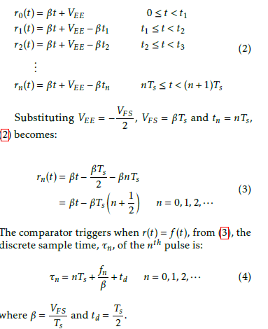
Conventional Pulse Position Modulation (PPM) generates one sample per period of a reference ramp [1]. In Substituting VEE = − VFS , VFS = βTs and tn = nTs, the PPM waveform generator circuit shown in Figure 1, f (t) is the input analog signal to be sampled and r(t) is a saw tooth reference waveform with period, Tramp. The comparator is assumed to be referenced from a positive voltage supply, VCC , and a negative supply
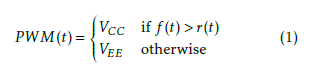
 voltage supply VEE. Pulse Width Modulation (PWM) is an ouput signal and PPM is the output Pulse Posi- tion Modulation signal generated by the monostable multivibrator (one shot) circuit. When triggered, a one shot produces a single pulse of fixed, finite duration. The comparator triggers when r(t) = f (t), from (3), the discrete sample time, τn, of the nth pulse is:
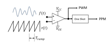 Figure 1: PPM Generator
A comparator, in general, will produce an output at the positive supply rail, VCC , whenever the signal input to the noninverting amplifier terminal, VⓍ+ , is greater than the signal input to the inverting amplifier terminal, VⓍ- . Similarly, the comparator output will be Equation (4) shows, in conventional PPM not only is the timing of the nth sample proportional to the sam- ple number, n, the timing is also a function of the signal being sampled. Consequently, it is seen, conventional PPM generates nonuniform sampling. at the negative supply rail, VEE, whenever VⓍ- > VⓍ+ . For the circuit in Figure 1, the PWM output signal as a function of time may be expressed as: otherwise Under the conditions specified, when r(t) exceeds f (t), the one shot will trigger and a sample generated. Assuming the bandwidth of the analog input, f (t), is
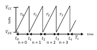 Figure 2: PPM Reference Ramp
3. ∆-PPM
Figure 3: Reset PPM GeneratorFigure 2 is an illustration of several cycles of the ref- erence ramp signal. In Figure 2, rn is the nth period of the reference signal. If we define the full scale voltage as, VFS = VCC VEE and let the negative supply rail be such that, VEE = VCC , as is typically the case, then we may write, VFS = 2VCC . We can then define the slope of the reference as, β = VFS . By direct enumeration, out explicitly having the PWM output trigger a one- shot. Such a direct generation of the PPM signal is accomplished by resetting the reference ramp after the comparator triggers. Generating a PPM signal by re- setting the reference ramp will be called, ∆ PPM, to distinguish it from conventional PPM. ∆ PPM may be generated with the circuit of Figure 3. In Figure 3, VCC and VEE are the power supplies for the comparator, f (t) is the signal to be sampled and r(t) is the reference ramp. Also shown in Figure 3 is a RESET circuit that asynchronously resets the reference ramp at each PPM pulse. Equation (7) shows, in ∆ PPM the timing of the n sample is a function of the signal being sampled
The previous periodicity of the reference signal is annihilated when the reference ramp is allowed to reset after the comparator triggers. An arbitrary response to the asynchronous triggering is shown in Figure 4. In and thus ∆ PPM generates nonuniform sampling, as in conventional PPM. Additionally, from (7), ∆ PPM samples times are a function of the previous sample time.
Two important consequence result if the sample times are a function of the previous sample time. First, Shapiro and Silverman [20] showed that sampling can be made alias free if each sample time is derived from the previous one by the addition of an independent ran- dom variable, from (7) it is seen that ∆ PPM provides such a sampling scheme. Second, Beutler [21] showed that if the sampling rate exceeds the Nyquist rate on av- erage then the nonuniform sampling set will be stable and can be used to reconstruct a band-limited signal. We now show that ∆ PPM produces a sampling set with an average sampling rate,Ravg , that approaches, Figure 4, we call rn is the nth response of the reference signal, rather than the nth period of the reference, and again define the full scale voltage as, VFS = VCC − VEE and the slope of the reference as, β = VFS . Using (7) iteratively we may write:
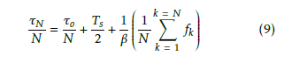
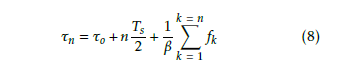 where τo is the first sampling instant. Let n N , be the total number of samples such that N : N 1, 2, 3, … and let τN be the maximum sample time, then, dividing by N:
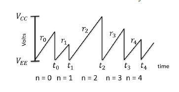 Figure 4: Reset PPM Reference Ramp
 By direct enumeration, rn(t) in Figure 4 is:
The last term in (9) is the average value of f (t). If the average value equals zero, then the average sample rate is given by:
 The maximum value of the first sampling instant is,
We note that the interval endpoints cannot be specified as constants, as was the case in conventional PPM, because they evolve dynamically. Again, substituting becomes: Less formally, for reasonable values of N experienced in practice, we may regard the average sample rate in
![]() The comparator triggers when r(t) = f (t), from (6), the discrete sample time, τn, of the nth pulse is:
The comparator triggers when r(t) = f (t), from (6), the discrete sample time, τn, of the nth pulse is:
The significance of (7) and (11) are that ∆ PPM is self-regulating. ∆ PPM automatically satisfies the Nyquist requirement on average (Beutler’s condition [21]) and produces alias free random sampling
 (Shapiro-Silverman condition [20]). Additionally,
∆ PPM achieves self-regulation with no a priori knowl- edge of the signal support and does not utilize any particular code or special sequence to generate random samples.
4. Geometric Partitioning
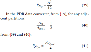
The stylized, equal partitioning, presented [1], was in- tended to provide an introduction for the essence of the PDR-ADC. We now develop the elaboration of the partitioning scheme, where significant benefits will be obtained.
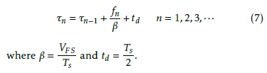
All data converters need an analog reference volt- age to accomplish the continuous to discrete transform and produce a digital word [22]. In general, the con- verter divides an analog reference voltage, VREF, into a fixed number of analog voltage levels, L. These analog voltage levels are then mapped to a digital number, typically referred to as counts. By convention, the smallest analog voltage level is assigned digital level 0 . The remaining analog voltage levels are mapped to digital levels by incrementing the ADC count. In this way, it is not possible to map the analog reference voltage, VREF, to a number that can be reached and assigned a digital count.
All of the digital levels taken together define the scale. In general, there will be L levels and L 1 steps. The reference voltage divided by the number of levels defines the size of the analog step to reach an adjacent level. The step size, ∆, is sometimes referred to as the quantization step size or the least significant bit (LSB). The maximum analog voltage that can be mapped to a digital level is called the full scale voltage, VFS . The re- lationship between the reference voltage, the full scale voltage and the quantization step size are shown in Figure 5 for a converter with L = 16 levels.
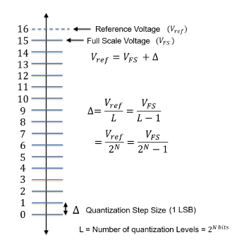 Figure 5: Quantization Step Size
The number of levels, L, is typically designed to be a function of the number of bits as, L = 2N , where N is the number of bits. For the 4 bit converter shown in Figure 5, the reference voltage is divided by 16 = 24.
The first digital level is assigned digital count 0 , and the digital number It is not possible to encode digital count 16 with a 4 bit counter, and con- sequently, the reference voltage, VREF in Figure 5, is not mapped to a digital number.
The principle of the geometric partitioning is shown in Figure 6 for a system with = 8 partitions and L = 4 levels. In the PDR data converter, the signal amplitude axis in partitioned into partitions such that each partition contains L levels, the partitions do not overlap and each partition has a different quantiza- tion step size. The geometric partitioning is achieved by relating the spans (the dynamic range) of the parti- tions as a geometric series.
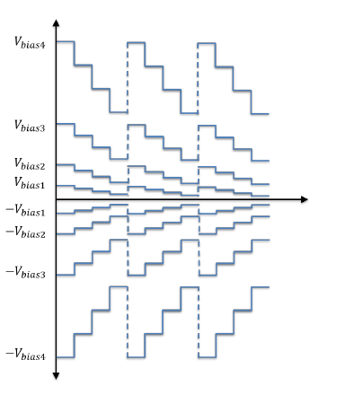 Figure 6: Geometric Partitioning: Conceptual
corresponds to the digital number. The maximum digital count is , and corresponds to
 Figure 7: Geometric Partitioning: Detail
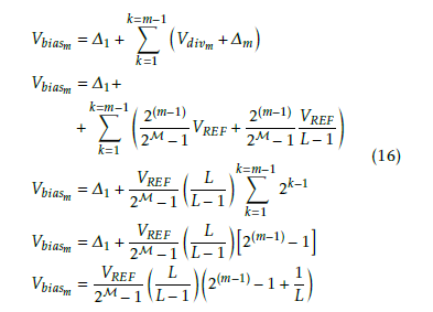
The relationship between partition bias voltages, Vbiasm , and the quantization step sizes needed to re- alize the behavior shown in Figure 6, can be better understood and visualized with the aid of Figure 7. Due to the symmetry of the bias voltages, only the pos- itive partitions, P1, P2, P3 and P4, as shown in Figure 7, are needed.
Let the total number of partitions, P , be even, and define the maximum partition number to be, = P , and let m denote the mth partition. In Figure 7, we denote by Vdivm the span of the m partition. By design, the spans of the partitions are geometrically related, thus:
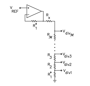 Figure 9: Step Compression Circuit
 To realize (12), a circuit that takes the output from the DAC and applies the appropriate gain to compress the DAC steps is required. The required step compres- sion response is shown in Figure 8 and the circuit to realize the response is shown in Figure 9.
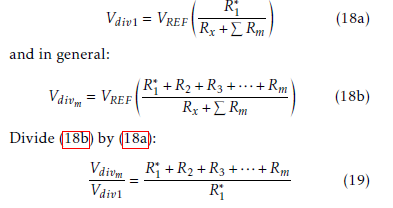
From (12) and (13), the mth voltage divider voltage is given by:
 Using Figure 7 and (14) and (15), we may write the bias voltages, Vbiasm , as:
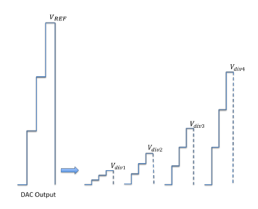 Figure 8: Step Compression Voltages
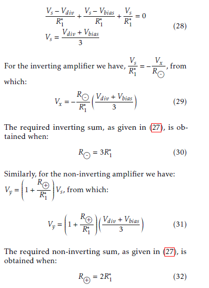
 The step compression circuit in Figure 9 is a non inverting voltage divider. To obtain design equations for the bias voltages in terms of the reference volt- the maximum number of partitions, M and the number of levels, L, we design the step compres- sion cir cuit such that the voltage drop across resistor,
Lastly, the Full Scale voltage shown in Figure 7 may Vdiv1. Then, due to the geometric be obtained by adding the results of (16) and (14) eval- design and Kirchoff’s voltage law, it must be the case: uating at m = M:
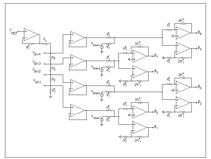 Figure 10: Step Compression & Level Shifting Circuit
In terms of the external design parameters, VREF, M and L, the number of partitions, M will have the and in general:
 since the bias is proportional to
5. Step Compression and Level Shifting
We now develop the circuit to generate the parallel digital ramps shown in Figure 6, and we call this function, step compression and level shifting (SCLS). The step compression and level shifting circuit is shown in Figure 10. Step compression is governed by equations
(14) and (15) and we seek now to determine design equations for the resistance for the circuit in Figure 10.
5.1. Step Compression
The step compression gains can be realized from circuit analysis by solving for the resistor values, in Figure 8, required to establish the voltage divider voltages,
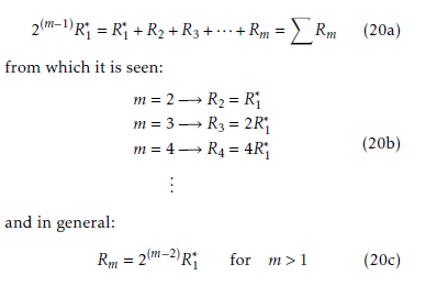
from which it is seen:
 Lastly, from Equation (13) and (18a):
The design is readily obtained if the inverting and noninverting amplifiers in 10 are solved with the feed- back resistors as arbitrary unknown resistors (2 de-
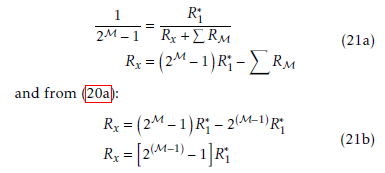 grees of freedom) and the remaining resistors fixed, and from (20a): equal to resistor R1∗ . A pair of inverting and noninvert- ing amplifiers are shown in Figure 11 where RⓍ- , is the resistor in the inverting amplifier and RⓍ+ is the resistor in the non-inverting amplifier.
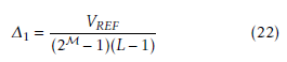
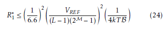
To complete the design of the Step Compression cir- cuit, we must specify a value for resistor R∗1. To do so, we seek a design equation that relates the RMS noise voltage of the resistor to the voltage of the smallest quantization step size, ∆1 in Figure 7. We then design
the resistor value be less than this value so that the system is limited by the quantization noise of the LSB rather than the thermal noise of the resistor.
From (15):
 Assuming the noise is Gaussian distributed, then approximately all of the noise is contained within 6.6 standard deviations1. The peak-to-peak thermal noise voltage of the resistor is given by:
![]() where R is the resistance in Ohms, k is Boltzmann’s
where R is the resistance in Ohms, k is Boltzmann’s
constant (k ≈ 1.30865×10⁻²³J/K), T is the temperature
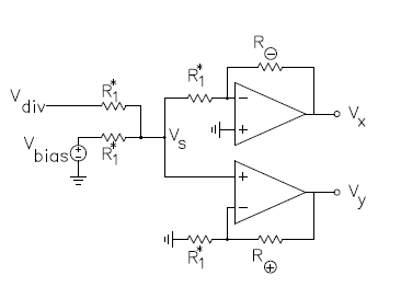 Figure 11: Level Shifting Feedback Scaling From circuit analysis, the node voltage, Vs is:
in Kelvin and B is the bandwidth in Hertz.
To design for the thermal noise voltage of R∗1 to be less than ∆1, we should select R∗1, such that:
 For the inverting amplifier we have, Vs = − Vx , from
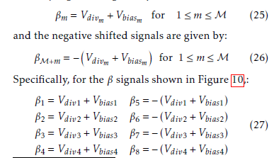
5.2. Level Shifting
Level shifting is governed by the bias voltages as given by (16). The aim of the level shifting circuit is to shift
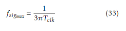
6. Maximum Sample Rate
input sinusoid of the form, f (t) = VFS sin(2πfsig t), the Samples are generated by the precision windowed dual maximum rate of change is: ∆V
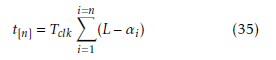
The slope edge detector shown in Figure 12. The edge detec- fastest rate of change the PDR can respond to is: tor triggers an asynchronous LOAD flip-flop that stores the instantaneous value of the counter to memory. The LOAD signal, additionally, “sets” an RS flip-flop that drives the synchronous RESET flip-flop. On the next CLOCK, Tclk, the RESET flip-flop resets the counter.
 The counter generates a HOLD OFF signal that inhibits additional LOAD signals until the counter has settled, where the safety time to settle is 1 CLOCK pulse. The sampling circuit is shown in Figure 12.
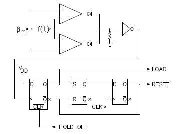 Figure 12: Windowed Synchronous One-Shot
7. The Counting Vector
In this section, we establish some important properties of the counting vector. Each intersection of f (t) with a reference counter step contributes to the counting vector, α. The counting vector is responsible for de- termining the time of each sample, the amplitude of each sample, and the number of samples acquired. The counting vector also contains the information about the number of missing samples and where these miss- ing samples are located. Information regarding the missing samples is critically important for reconstruc- tion as the location and number of the missing samples (the data to be interpolated) must be known.
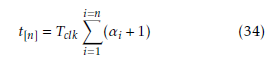
We denote by α, the number of counts accumulated by the counter. If the counter is strictly counting up, then the time to accumulate α counts, tα = (α + 1)Tclk, where Tclk is the clock period. The time of the nth sample, t[n], is the cumulative sum of the tα’s: In the PDR data converter, we must ensure that
 the counter has settled before the next LOAD/RESET cycle. The worst case signaling (fastest signal) corre- sponds if the LOAD signal aligns with a CLOCK edge. In such a case, a minimum of 3 CLOCKS is required to guarantee correct conversion before the next LOAD signal is allowed to register a new sample, this worst
If, instead, the counter is strictly counting down, we denote by αc (the complement of α) the number of counts accumulated by the counter. In this way, αc = (L 1) α, where L 1 is the maximum value of the counter. In this case, the time of the nth sample is:
case timing is shown in Figure 13.
 The direction of the counter can be changed, by using a toggle flip-flop clocked on each RESET signal, and the system will continue to maintain the correct timing of each sample.
To recover the signal requires a method to resolve the counter slope, the partition number and the count value. We append, to the counting vector, additional bits that correspond to the counter slope and the parti- tion number. As a specific example of accommodating partition encoding, suppose a PDR-ADC is designed with = 8 partitions and L = 256 levels per partition. The partition encoder requires 3 bits, the count slope requires 1 bit and the count value requires 8 bits, the data word stored in memory will be of the form:
 Figure 13: LOAD/RESET Timing
To determine the maximum signal frequency that the PDR-ADC can accommodate, we equate the max- imum rate of change of the input signal, to the max- imum rate of change allowable by the PDR. With an
Slope Partition number
| B12 | B11 | B10 | B9 |
| B8 | B7 | B6 | B5 | B4 | B3 | B2 | B1 |
In this example, the partition number in each data word is determined by:
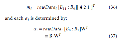 where, W = [ 128 64 32 16 8 4 2 1 ].
In general, once the ith partition number, mi , and the ith count, αi , have been determined, the sampled voltage value is given by:
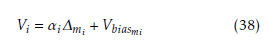
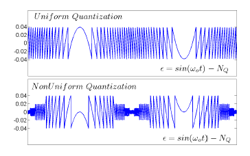 Figure 14: Quantization Error Comparison
Now suppose a signal of the form, y = Ao sin(ω t) is input to this uniform quantizer, the SQNR becomes:
Lastly, since α + 1 is the number of clocks to obtain
 αi counts, then αi is equal to the number of missing samples if the signal had been sampled at a rate equal to Tclk.
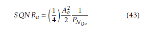
8. Signal to Quantization Noise Ra- tio (SQNR)
From (42) and (43), in a uniform quantizer, when the input signal amplitude decreases by a factor of 2, the SQNR degrades by a factor of 4.
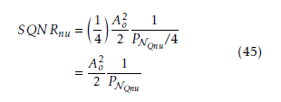
Now consider a signal of the form, y = Aosin(ωot), input to the nonuniform PDR quantizer with quantiza- tion noise power, PNQnu , the SQNR is given by:
The signal to noise ratio (SNR) is always equal to the ratio of the signal power, Psig , to the noise power, PNQ .
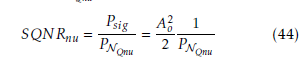 In data converters, the “noise” added by the system due to the act of approximating (truncating) a continue Again, suppose the input signal amplitude decreases by a factor of 2 and let y = Ao sin(ω t) be input to the function to finite precision is quantization noise, and the ratio of interest is the signal to quantization nonuniform PDR quantizer, then, by (41), the SQNR noise, SQNR = Psig /PNQ . In uniform quantizers, the becomes: quantization noise power is well approximated by, [17],
 In the PDR data converter, from (15), for any adjacent partitions:
 From (44) and (45), it is seen, the geometric partition- ing of the PDR-ADC attempts to maintain the signal-to- quantization noise ratio constant, this is a significant improvement compared to uniform quantization data converters.
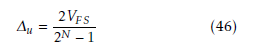
We shall now be concerned with determining this constant. In an N bit uniform quantizer, the quantization step size, ∆u
For the PDR, (41) states, the quantization noise power decreases by a factor of 4 when transitioning
 from a higher partition to a lower level partition. This effect is shown in the bottom panel in Figure 14, where, for comparison, we have also plotted the quantization error of a uniform quantizer in the top panel.
Let a signal of the form, y = Aosin(ωot), be input Suppose we have a PDR data converter, with max- imum partition number, , and L = 2N levels per partition, where N is the same as the uniform quan- tizer in (46). In the PDR, the largest quantization step size is given by (15), evaluated at m = M. to a uniform quantizer with quantization noise power,
PNQu , the SQNR is given by:
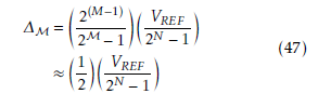
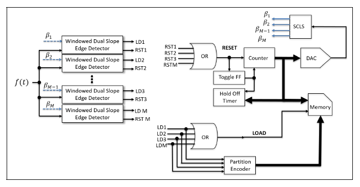 Figure 15: Parallel Digital Ramp ADC Overall Block Diagram
Using (46), we may write (47) as:
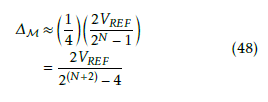 In a PDR data converter, with L = 2N levels per parti- tion, (48) states, the PDR has gained approximately 2 bits of resolution compared to a uniform quantizer.
The results of (45) and (48) may be summarized as, given a PDR data converter with L = 2N levels, the SQNR of the system will be approximately equivalent to a uniform system with L = 2(N+2) levels and the PDR will attempt to maintain this performance for all input signal levels.
9. Simulation Results
The proposed parallel digital ramp ADC was modeled and simulated in SimulinkⒹ and the reconstruction performed in MatlabⒹ. The overall block diagram of the new ADC is shown Figure 15.
9.1. Linearity
The linearity of the PDR was analyzed empirically us- ing a triangle wave, as shown in Figure 16, since, by design, the sampled data is not equally spaced. This approach was taken because the data converter figure of merit, Differential Non-Linearity (DNL), is a func- tion of the difference of consecutive samples with a constant step size, as given by (49), where for an ideal ADC, the DNL = 0 [18]. In the PDR, since large gaps appear in the data and the step size is not constant, linearity is more easily performed graphically.
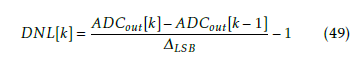
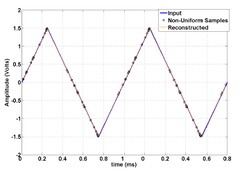 Figure 16: Reconstructed Linear
9.2. Electrocardiogram (ECG) Reconstruc- tion
To test the new PDR data converter to acquire and reconstruct an analog signal from its nonuniform sam- ples, a simulated electro-cardiogram (ECG) signal [25] was used. These signals have a wide dynamic range and “contain the QRS complex, which ensures oscilla- tions near the Nyquist rate” [26] and are thus useful in exercising the nonuniform sampling architecture of the PDR.
The simulated ECG signal was modeled with a 1mV peak amplitude with 0.3mV DC offset and zero mean Gaussian noise with noise variance σ o 0.058nW was added to the signal.
A wide view of the simulated run time of 10 sec- onds is shown in Figure 17, which demonstrates the PDR’s ability to maintain the count. A zoom view of the reconstructed signal is shown in Figure 18, high- lighting the features of the QRS pulse. When the signal is “idle” (DC like), and loiters near 0 Volts, the system continues to generate samples and is not adversely affected by the lack of signal dynamics.
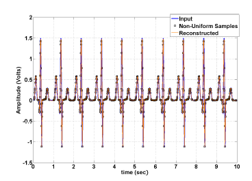 Figure 17: Reconstructed (simulated) ECG: Wide View
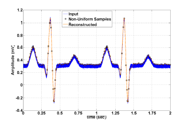 Figure 18: Reconstructed (simulated) Noisy ECG: Zoom View
10. Conclusion
A novel Analog-to-Digital Converter architecture based on partitioning the signal amplitude axis as a ge- ometric series has been described. A detailed analysis of the design requirements to achieve the geometric partitioning has been provided and the essential cir- cuits to realize the design presented. To extract the information content in each nonuniform digital sam- ple, a proposed format of the nonuniform data was established, where it was shown that the partition num- ber must be included in the digital word. Using reset ∆ PPM was shown to cause the system to satisfy the Nyquist requirement on average, and the geometric partitioning was shown to cause the SQNR to attempt to remain approximately constant. Lastly, the linearity of the PDR and the reconstruction of a simulated ECG signal were illustrated through simulation.
Conflict of Interest
The authors declare no conflict of interest.
- C. Pappas, “A New Non-Uniform ADC: Parallel Digital Ramp Pulse Positino Modulation” in 31st IEEE Canadian Conference on Electrical and Computer Engineering (CCECE), Quebec Canada, May 2018. https://doi.org/10.1109/CCECE.2018.8447844
- S. Maymon, A. Oppenheim, “Sinc Interpolation of Nonuniform Samples” IEEE T SIGNAL PROCES, 59(10), 4745–4758, 2011. https://doi.org/10.1109/TSP.2011.2160054
- D. Donoho, P. Stark, “Uncertainty Principles and Signal Recovery” SIAM J. Appl. Math., 49(3), 906–931, 1989. https://doi.org/10.1137/0149053
- E. Candes, T. Tao, “Near-Optimal Signal Recovery from Random Projections: Universal Encoding Strategies?” IEEE T INFORM THEORY, 52(12), 5406–5425, 2006. https://doi.org/10.1109/TIT.2006.885507
- Y. Eldar, G. Kutyniok, Compressed Sensing Theory and Applications, Cambridge University Press,2012.
- F. Marvasti, Nonuniform Sampling Theory and Practice, Kluwer Academic/Plenum Publishers, 2001.
- J. Mark, T. Todd, “A Nonuniform Sampling Approach to Data Compression” IEEE T COMMUN, 29(1), 24–32, 1981. https://doi.org/10.1109/TCOM.1981.1094872
- N. Sayiner, H. Sorensen, T. Viswanathan, “A Level-Crossing Sampling Scheme for A/D Conversion” IEEE T CIRCUITS SYST, 43(4), 335–339, 1996. https://doi.org/10.1109/82.488288
- E. Allier, J, Goulier, G. Sicard, A. Dezzani, E. Andre, M. Renaudin, “A 120nm Low Power Asynchronous ADC” in ISLPED ’05. Proceedings of the 2005 International Symposium on Low Power Electronics and Design, San Diego USA, 2005. https://doi.org/10.1145/1077603.1077619
- T. Wang, D. Wang, P. Hurst, B. Levey, S. Lewis, “A Level-Crossing Analog-to-Digital Converter with Triangular Dither” IEEE T CIRCUITS SYST, 56(9), 2089–2099, 2009. https://doi.org/10.1109/TCSI.2008.2011586
- M. Malmirchegini, M. Kafashan, M. Ghassemian, F. Marvasti, “Non-uniform sampling based on an adaptive levelcrossing scheme” IET SIGNAL PROCESS, 9(6), 484–490, 2015. https://doi.org/10.1049/iet-spr.2014.0170
- S. Qaisar, M. Ben-Romdhane, O. Anwar, MTlili, A. Maalej, F. Rivet, C. Rebai, D. Dallet, “Time-domain characterization of a wireless ECG system event driven A/D converter” in 2017 IEEE International Instrumentation and Measurement Technology Conference (I2MTC), Turin Italy, 2017. https://doi.org/10.1109/I2MTC.2017.7969682
- S. Naraghi, “Time-Based Analog to Digital Converters”, Ph.D Thesis, University of Michigan, 2009.
- P. Maechler, N. Felber, A. Burg, “Random Sampling ADC for Sparse Spectrum Sensing” in 2011 19th European Signal Processing Conference, Barcelona Spain, 2011.
- S. Becker, “Practical Compressed Sensing: Modern Data Acquisition and Signal Processing”, Ph.D Thesis, California Institute of Technology, 2011.
- M. Wakin, S. Becker, E. Nakamura, M. Grant, E. Sovero, D. Ching, J. Yoo, J. Romberg, A. Emami-Neyestanak, E. Candes, “A Nonunifom Sampler for Wideband Spectrally-Sparse Environments” IEEE J EM SEL TOP C, 2(3), 516–529, 2012. https://doi.org/10.1109/JETCAS.2012.2214635
- R. Gray, D. Neuhoff “Quantization” IEEE T INFORM THEORY, 44(6), 2325–2383, 1998. https://doi.org/10.1109/18.720541
- W. Kestler (Editor), The Data Conversion Handbook, Analog Devices Inc., Elsevier-Newnes, 2005.
- C. E. Shannon, “Communication in the Presence of Noise” Proceedings of the IRE, 37(1), 10–21, 1949. https://doi.org/10.1109/JRPROC.1949.232969
- H. Shapiro and Richard A. Silverman, “Alias-Free Sampling of Random Noise”, New York University – Institute of Mathematical Sciences, 1959.
- F. Beutler, “Error-Free Recovery of Signals from Irregularly Spaced Samples” SIAM J. Appl. Math., 8(3), 328–335, 1966. https://doi.org/10.1137/1008065
- R. Baker, H. Li, and D. Boyce, CMOS Circuit Design, Layout and Simulation, IEEE Press Series on Microelectronic Systems, Wiley Interscience, 1998.
- W.R. Bennett, “Spectra of Quantized Signals” Bell Sys. Tech. Journal, 27(3), 446–472, 1948. https://doi.org/10.1002/j.1538- 7305.1948.tb01340.x
- Subbarayan Pasupathy, Minimum Shift Keying: A Spectrally Efficient Modulation, IEEE Communications Magazine, Vol: 17, Issue: 4, July 1979
- Sophocles J. Orfanidis, Introduction to Signal Processing, Pearson Education/Prentice Hall, 1996.
- Marco A. Gurrola-Navarro, “Frequency-Domain Interpolation for Simultaneous Periodic Nonunifom Samples” in 2018 IEEE 9th Latin American Symposium on Circuits and Systems (LASCAS), Puerto Vallarta Mexico,, 2018. https://doi.org/10.1109/LASCAS.2018.8399937